
Abstract
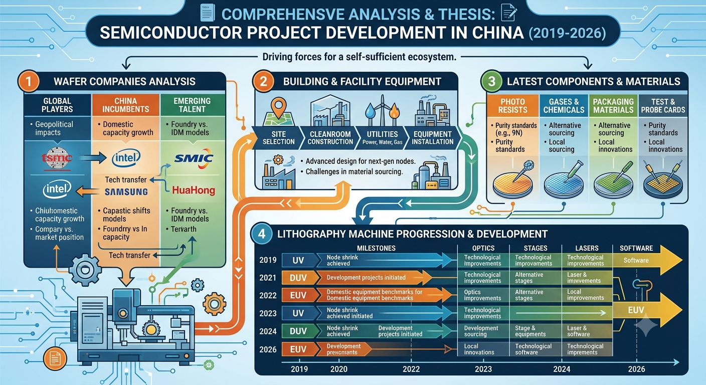
From 2019 to 2026, China’s semiconductor industry shifted from importing tools to building a domestic ecosystem. Driven by U.S. export controls, Chinese wafer companies and equipment makers accelerated development in lithography, etch, deposition, and process control. While a gap remains with ASML and TSMC, China has achieved functional DUV immersion, scaled domestic equipment supply, and set targets for EUV by 2030.
1. The Landscape: Wafer Companies and Fabs Leading China
Core Wafer Manufacturers
- SMIC – China’s largest foundry. Testing domestic tools and pushing 7nm/5nm via DUV multi-patterning. Founder Zhang Rujing stated SMIC bought 800+ machines from AMEC.
- Hua Hong, CXMT, YMTC – Focus on mature nodes, memory, and power. Beneficiaries of domestic equipment scale-up. 3b5462c0
China has been the world’s biggest buyer of wafer fab equipment for 2 years. In 2024 it purchased $41 billion, 40% of global sales. 4009
2. Building Equipment: The Domestic Ecosystem 2019-2026
Export controls starting in 2019 forced localization. By 2026 Chinese suppliers cover almost every process step: deposition, etch, cleaning, metrology. f572
Key Chinese Equipment Companies:
Company | Focus | Progress 2019-2026
NAURA Technology | Etch, PVD, CVD, furnace, cleaning | Largest domestic equipment maker. Revenue 29.8B yuan in 2024, 5x vs 2020
AMEC | CCP/ICP etch, TSV, MOCVD | Covers 30% of IC equipment categories. Aims for 60% in 5-10 years. Etch tools now support 5nm/3nm
SMEE | Lithography DUV | Most advanced: SSA600 90nm. Developing SSA800 28nm, SSA900 22nm
Yuliangsheng / SiCarrier | Immersion DUV, future EUV | Delivered 3 DUV immersion tools to fabs. Working on EUV “Mount Everest”
ACM Research, Hwatsing, Kingsemi, Piotech | Cleaning, CMP, track, ALD | Top 30 global equipment suppliers
4009f57262c09cc73b54f78f
Self-sufficiency for 7nm and below equipment is still <10%, but for cleaning and resist removal it’s ∼50%. 4009
3. Lithography Machine Progression: The Core Bottleneck
Lithography “prints” circuits on wafers. This is where China faced the hardest block.
The External Constraint
- 2019: US began restricting ASML EUV sales to China.
- 2023: US also blocked advanced immersion DUV.
- ASML remains the only EUV maker, $300M per machine, shipping 60 in 2026 and 80 in 2027. 40094d87
China’s Domestic Response
Phase 1: 2019-2022 – Rely on Old DUV
Fabs used older ASML DUV, second-hand imports, and SMEE 90nm tools. SMEE SSA600 = 90nm resolution. f78f9cc7
Phase 2: 2023-2025 – Immersion DUV Breakthrough
SMIC began testing Yuliangsheng’s domestic immersion DUV in 2024-2025.
- Specs: 28nm-class single exposure.
- Capability: With multi-patterning can reach 7nm, possibly 5nm at low yield.
- Cost/Yield issue: SMIC 5nm wafers via DUV may cost 50% more than TSMC with yields as low as 33%.
- Supply chain: Mostly Chinese parts, but some still imported. Goal is full localization.
- Benchmark: Similar to ASML NXT:1950i from 2008, designed for 32nm. 73c63b5434c4
Phase 3: 2026-2030 – Targeting EUV
- SMEE: Developing SSA800 28nm, SSA900 22nm.
- SiCarrier/Yuliangsheng: Working on China’s first EUV tool codenamed “Mount Everest”.
- Analyst view: Even if SMIC integrates 28nm immersion DUV by 2027, sub-10nm will need redesigned scanners and likely won’t be domestically made before 2030. 9cc7f78f3b54
4. Latest Components in Semiconductor Projects
A modern fab needs 3,000+ tools. China’s 2019-2026 build-out focused on: 4009
A. Patterning: SMEE DUV, Yuliangsheng immersion DUV. EUV still in R&D.
B. Etch: AMEC’s VHF decoupled plasma etch, supporting 5nm/3nm.
C. Deposition: NAURA CVD/PVD/ALD, AMEC MOCVD gaining global share.
D. Cleaning/Wet: ACM Research, Kingsemi.
E. Metrology/Inspection: Raintree Scientific.
F. CMP and Edge Polish: Hwatsing. 62c03456
AMEC aims to complete 20 types of restricted thin-film equipment soon, and 40 by 2029. f572
5. Significance and Challenges
Significance
- Self-reliance: The 2019 sanctions catalyzed a domestic supply chain. Gap with leaders is “continuously narrowing”.
- Scale: China’s fab spending dominance funds local equipment makers.
- Technology: Breakthroughs in immersion DUV and etch show capability to replicate, then iterate. f572
Challenges
- Lithography gap: Still 2-3 generations behind ASML. No EUV in production.
- Yield and cost: DUV multi-patterning for 7nm/5nm is expensive and low yield.
- Components: Some critical lenses, lasers, optics still imported. f5723b544d87
6. Conclusion: 2019-2026 as a Foundational Era
2019-2026 was not about catching ASML in EUV. It was about survival and building the base.
China moved from <20% equipment coverage to near-complete process coverage except advanced lithography. SMIC’s testing of domestic immersion DUV and the emergence of NAURA, AMEC, SMEE in the global top 30 signal this shift. 73c6f572
The next 5 years will determine if “Mount Everest” EUV and SSA800/900 DUV can close the gap for sub-7nm. For now, China’s strategy is: dominate mature nodes with domestic tools, and use DUV ingenuity to push advanced nodes until EUV arrives.
As analyst Lin Qingyuan put it: if successful, this breakthrough lets Chinese companies build more advanced machinery. f78f
Comprehensive Analysis and Thesis
China’s Semiconductor Industry (2019–2026): Wafer Companies, Manufacturing Equipment, Components, and Lithography Machine Development
Executive Summary
Between 2019 and 2026, China’s semiconductor industry underwent one of the fastest industrial transformations in modern history. Triggered by export controls, supply-chain disruptions, and the strategic goal of semiconductor self-sufficiency, China invested hundreds of billions of yuan into virtually every layer of the semiconductor ecosystem—from silicon wafers and fabrication equipment to electronic design automation (EDA), process chemicals, advanced packaging, and lithography.
Despite substantial progress, China has not yet achieved full independence in the most advanced semiconductor technologies. Strong gains have occurred in mature-node manufacturing, etching, deposition, cleaning, and wafer production, while EUV lithography remains beyond commercial domestic capability. DUV lithography, advanced packaging, and mature-node fabrication have become major strengths. (South China Morning Post)
Chapter 1
China’s Semiconductor Ecosystem
The semiconductor industry consists of several interconnected sectors:
| Sector | Purpose |
|---|---|
| Silicon wafers | Base material for chips |
| Semiconductor equipment | Machines that manufacture chips |
| Lithography | Printing transistor patterns |
| Deposition | Thin-film creation |
| Etching | Material removal |
| Cleaning | Surface preparation |
| Metrology | Measurement |
| Inspection | Defect detection |
| CMP | Surface polishing |
| Packaging | Final chip assembly |
| Testing | Functional verification |
| Materials | Chemicals, gases, photoresists |
China invested heavily across all of these sectors after 2019.
Chapter 2
Major Chinese Silicon Wafer Companies
China significantly expanded domestic silicon wafer production.
1. Shanghai Silicon Industry Group (NSIG)
Produces:
- 300 mm wafers
- 200 mm wafers
- SOI wafers
- Epitaxial wafers
Applications:
- AI chips
- Automotive chips
- Memory
- Power electronics
2. Zhonghuan Semiconductor
Specializes in:
- Large-diameter silicon crystals
- Integrated circuit wafers
- Solar-grade silicon
3. GRINM Semiconductor
Focus:
- Compound semiconductor substrates
- Gallium arsenide
- Indium phosphide
4. Simgui Technology
Manufactures:
- SOI wafers
- MEMS wafers
- RF device substrates
5. National Silicon Industry Group
Develops:
- 12-inch wafers
- Advanced silicon materials
- High-purity crystal growth
China has set ambitious localization targets for silicon wafers, reflecting its broader supply-chain strategy. (The Economy)
Chapter 3
Semiconductor Equipment Manufacturers
China has rapidly developed domestic suppliers across many equipment categories.
Major companies include:
- Naura Technology Group
- AMEC (Advanced Micro-Fabrication Equipment)
- SMEE (Shanghai Micro Electronics Equipment)
- Piotech
- Kingsemi
- ACM Research (China operations)
- Hwatsing Technology
- Kingsemi Equipment
- Beijing E-Town Semiconductor
These firms now compete in etching, deposition, cleaning, polishing, packaging, and certain lithography applications. (South China Morning Post)
Chapter 4
Wafer Fabrication Equipment
Modern chip factories require hundreds of specialized machine types.
Core categories include:
Front-End
- Crystal pullers
- Wafer slicing
- Grinding
- Polishing
- Cleaning
Lithography
- Stepper
- Scanner
- Mask aligner
- Overlay systems
Deposition
- CVD
- PVD
- ALD
- Epitaxy
Etching
- Dry etching
- Plasma etching
- ICP etching
- Reactive ion etching
Cleaning
- Megasonic cleaning
- Wet benches
- Single-wafer cleaning
Implantation
- Ion implantation
- Dopant activation
Thermal Processing
- Rapid thermal annealing
- Diffusion furnaces
- Oxidation furnaces
CMP
- Chemical mechanical polishing
- Slurry systems
- Pad conditioning
Inspection
- Optical inspection
- Electron beam inspection
- Defect review
Metrology
- CD measurement
- Film thickness
- Overlay accuracy
Chapter 5
Components Inside Semiconductor Manufacturing Equipment
Every semiconductor machine contains numerous precision subsystems:
- Industrial robots
- Vacuum chambers
- Laser systems
- Precision optics
- Motion stages
- Air bearings
- Magnetic levitation
- Piezo actuators
- Wafer handling robots
- Gas delivery systems
- High-vacuum pumps
- RF plasma generators
- Temperature controllers
- CCD/CMOS cameras
- X-ray systems
- Spectrometers
- AI control computers
- Industrial PLCs
- Edge computing controllers
- Ultra-pure water systems
- Chemical delivery modules
- Electrostatic chucks
- Power supplies
- Servo motors
- Linear motors
- Nanometer positioning systems
- Cleanroom enclosures
- HEPA filtration
- Optical sensors
- Metrology software
- Machine-learning process optimization
Chapter 6
Lithography Machine Evolution (2019–2026)
Lithography is the most technologically demanding step in semiconductor fabrication.
2019
China relied largely on imported DUV systems. EUV lithography systems from the Netherlands were not available due to export restrictions.
2020
Chinese companies intensified research into:
- Precision optics
- Laser sources
- Motion control
- Optical stages
- Alignment systems
2021
SMEE continued development of domestic lithography platforms, with commercial strengths in packaging, MEMS, LED, and mature-node applications while pursuing more advanced DUV capabilities. (Semiconductor Expo)
2022
Investment accelerated in:
- Precision mirrors
- Lens polishing
- Motion stages
- Photoresist chemistry
- Mask technology
2023
Domestic development expanded in:
- Immersion lithography research
- Advanced packaging lithography
- High-precision alignment
- Overlay improvement
2024
China strengthened:
- Optical component manufacturing
- Laser systems
- High-precision manufacturing
- Domestic supply chains
2025
Chinese equipment makers significantly increased their share of domestic semiconductor equipment purchases, especially in etching and deposition. Reports indicated domestic equipment adoption exceeded government targets in several segments. (South China Morning Post)
2026
China continues to commercialize more domestic semiconductor equipment across mature and some advanced manufacturing processes. Public evidence indicates continued progress in DUV-related technologies and equipment localization, but there is no verified evidence that China has commercially deployed a domestically produced EUV lithography machine. Advanced lithography remains an area where foreign technology leadership persists. (The Economy)
Chapter 7
Lithography Progression
| Generation | Approximate Wavelength | Typical Use |
|---|---|---|
| Contact lithography | 365 nm | Early ICs |
| i-line | 365 nm | Mature processes |
| KrF | 248 nm | Legacy logic |
| ArF Dry | 193 nm | Mid-generation nodes |
| ArF Immersion | 193 nm | Advanced DUV |
| Multiple Patterning | 193 nm | Extends DUV capability |
| EUV | 13.5 nm | Leading-edge nodes |
Chapter 8
Major Technological Challenges
China continues to face challenges in:
- EUV light sources
- Ultra-precision mirrors
- High-NA optics
- Advanced photoresists
- Precision mask manufacturing
- Defect-free optics
- Nanometer-level positioning
- Advanced metrology
- High-end inspection systems
These areas remain among the most difficult parts of the semiconductor manufacturing ecosystem. (The Economy)
Chapter 9
Areas of Rapid Progress
China has made notable advances in:
- Silicon wafer manufacturing
- Etching systems
- Deposition equipment
- Cleaning equipment
- CMP equipment
- Packaging
- Testing
- Industrial robotics
- Process automation
- AI-assisted manufacturing
- Compound semiconductors
- Power semiconductor production
Chapter 10
Future Outlook (2026–2035)
Likely areas of continued development include:
- Higher domestic equipment adoption
- Improved 300 mm wafer production
- More advanced DUV lithography
- Greater use of AI in process control
- Expanded advanced packaging (2.5D and 3D integration)
- Improved metrology and inspection capabilities
- Continued investment in domestic supply chains
At the same time, leading-edge EUV lithography and some of the most advanced semiconductor manufacturing technologies are expected to remain technically challenging and highly competitive globally.
Conclusion
From 2019 to 2026, China’s semiconductor industry evolved into one of the world’s largest and fastest-growing ecosystems. Domestic firms achieved major gains in wafer production, etching, deposition, cleaning, packaging, and mature-node manufacturing. Government investment and localization policies accelerated adoption of Chinese-made equipment, increasing domestic market share substantially. However, the industry still relies on foreign technology in several critical areas—particularly advanced lithography, high-end metrology, and inspection—making these the next major frontiers for China’s semiconductor ambitions. (South China Morning Post)





Be First to Comment