
Architecture, Principles, Scientific Applications, and Tutorial
Comprehensive Thesis
Правила роботи з світловим мікроскопом
9
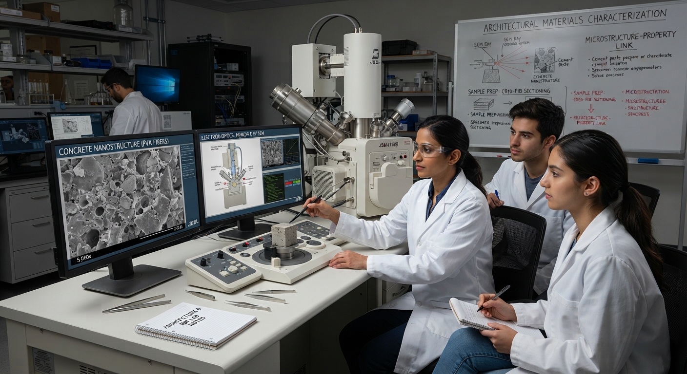
Electron microscopy (EM) is one of humanity’s most powerful technologies for investigating the microscopic and nanoscopic world. It allows scientists to examine structures far smaller than those visible with ordinary optical microscopes—including viruses, cellular organelles, molecular assemblies, semiconductor structures, nanoparticles, and the fine architecture of materials.
Its significance lies in its ability to transform invisible structures into measurable scientific information.
Chapter 1 — Introduction to electron microscopy
1.1 What is electron microscopy?
Electron microscopy is a technology that uses a beam of electrons rather than visible light to illuminate, scan, or pass through a specimen.
An ordinary optical microscope uses photons and glass lenses. An electron microscope uses:
- Electron sources
- High-voltage acceleration systems
- Electromagnetic lenses
- Vacuum chambers
- Specimen stages
- Electron detectors
- Digital imaging and computational analysis
Electrons behave as particles and also exhibit wave properties. Their wavelength can be much shorter than visible light, enabling extremely high-resolution imaging.
The fundamental difference
| Technology | Illumination | Main lens system | Typical scale |
|---|---|---|---|
| Optical microscope | Visible light | Glass lenses | Micrometers |
| Electron microscope | Electron beam | Electromagnetic lenses | Nanometers |
| Advanced electron microscopy | Accelerated electrons | Precision electromagnetic optics | Atomic-scale imaging in suitable conditions |
The smaller wavelength of accelerated electrons is one of the fundamental reasons electron microscopy can reveal much finer detail than conventional optical microscopy.
Chapter 2 — The physics behind electron microscopy
2.1 Electrons and wave-particle duality
An electron is a subatomic particle carrying a negative electrical charge.
When electrons are accelerated through an electrical potential, they gain kinetic energy.
The relationship between electron momentum and wavelength is described by the de Broglie equation:
\[ \lambda=\frac{h}{p} \]
Where:
- \(\lambda\) = electron wavelength
- \(h\) = Planck’s constant
- \(p\) = momentum
For electrons accelerated through a voltage, their wavelength becomes extremely short.
For example, at an accelerating voltage of 100 kV, the relativistic electron wavelength is approximately:
\[ \lambda\approx3.7\text{ picometers} \]
That wavelength is much smaller than the spacing between many atoms.
However, having a very short wavelength does not automatically guarantee atomic-resolution images. The quality of the final image also depends on lens aberrations, vibration, specimen stability, electron scattering, detector performance, and signal processing.
2.2 Why electrons must be accelerated
An electron source produces electrons.
An electrical field accelerates them toward the microscope’s optical system.
The accelerating voltage determines their energy.
Basic electron acceleration
\[ E_k\approx eV \]
Kinetic energy is approximately equal to the electron charge multiplied by the accelerating voltage.
For example:
- 1 kV = 1,000 electron-volts per electron
- 10 kV = 10,000 electron-volts
- 100 kV = 100,000 electron-volts
- 300 kV = 300,000 electron-volts
Higher voltage generally provides electrons with greater penetrating ability, but the appropriate voltage depends on the specimen and imaging technique.
Chapter 3 — The complete architecture of an electron microscope
6.7 : Dualité onde-particule – Global
Cryo electron microscopy | PPTX
8
The architecture can be understood as a vertical scientific instrument that controls electron generation, acceleration, focusing, specimen interaction, and signal collection.
3.1 The major subsystems
1. Electron source
Produces electrons
2. Acceleration system
Establishes electron energy
3. Condenser lenses
Controls beam illumination
4. Specimen chamber
Electron beam interacts with specimen
5. Objective lens
Creates the initial image or diffraction pattern
6. Imaging and analytical systems
Magnification, scanning, spectroscopy, and signal collection
7. Detector and computer
Converts electron signals into digital information
3.2 Electron source
The electron gun is the beginning of the electron optical system.
Its function is to produce a controlled stream of electrons.
Common electron sources include:
A. Thermionic emission
A material is heated sufficiently for electrons to escape its surface.
Typical source materials include tungsten and lanthanum hexaboride (LaB₆).
Advantages include relatively simple construction and established technology.
B. Field emission
Strong electric fields help electrons escape from a very small emitting region.
Field-emission sources can provide:
- High brightness
- Small electron-source size
- High spatial coherence
- Improved fine-detail imaging
Different field-emission configurations include cold field emission and thermally assisted field emission.
Chapter 4 — Electron lenses and beam control
Unlike ordinary optical microscopes, electron microscopes use electromagnetic fields to control electron trajectories.
4.1 Condenser lenses
Condenser lenses control:
- Beam diameter
- Illumination intensity
- Beam convergence
- Electron current reaching the specimen
The specimen must receive an electron beam with suitable characteristics for the chosen experiment.
4.2 Objective lens
The objective lens is one of the most important components.
It strongly influences:
- Image formation
- Resolution
- Focus
- Contrast
- Magnification characteristics
The objective lens interacts with electrons after they have passed through or interacted with the specimen.
4.3 Intermediate and projector lenses
In many transmission electron microscopes, additional electromagnetic lenses magnify the intermediate image to create a final image.
The microscope’s total magnification is approximately the product of the magnification stages:
\[ M_{\text{total}}=M_1\times M_2\times M_3 \]
For example, three imaging stages with magnifications of 10×, 20×, and 50× produce:
\[ 10\times20\times50=10,000\times \]
Actual microscope magnification may involve different optical configurations, digital scaling, and calibrated image recording.
Chapter 5 — The two principal electron microscopy technologies
The two most widely recognized electron microscopy systems are:
- Transmission Electron Microscopy (TEM)
- Scanning Electron Microscopy (SEM)
Although both use electrons, they create images in different ways.
5.1 Transmission Electron Microscope (TEM)
Back to School: What Mitochondria Really Do | Yale School of Medicine
细胞–中国科学院生物物理研究所蛋白质科学研究平台生物成像中心
10
A TEM sends electrons through a very thin specimen.
Some electrons pass through relatively easily, while others are scattered or absorbed. These differences produce contrast that can reveal internal structures.
TEM architecture
Electron source
Condenser optical system
Thin specimen
Objective lens
Intermediate and projector lenses
Electron detector
What TEM can reveal
- Internal cell structures
- Mitochondrial membranes
- Ribosomes
- Cellular membranes
- Viral structures
- Crystal lattices
- Nanoparticles
- Semiconductor layers
- Defects in materials
- Atomic arrangements under suitable conditions
TEM image interpretation
A TEM image is often a two-dimensional projection of a three-dimensional specimen.
Dark regions may indicate stronger scattering or absorption of electrons. Bright regions may indicate that more electrons reached the detector.
Contrast depends on specimen composition, thickness, orientation, imaging conditions, and detector configuration.
5.2 Scanning Electron Microscope (SEM)
Mathew Schwartz (@cadop) | Unsplash Photo Community
SEM-Insects Image 14 — Erwin Huebner | Scientist | Artist
12
SEM works by scanning a focused electron beam across the surface of a specimen.
Rather than primarily forming an image from electrons transmitted through a thin specimen, SEM collects signals generated by interactions between the beam and the specimen.
SEM architecture
Electron source
Beam focusing system
Scanning coils
Specimen surface
Signal generation
Electron detectors
Digital image reconstruction
SEM signals
When the electron beam interacts with a specimen, several types of signals may be generated.
Secondary electrons
Useful for surface detail and topography.
Backscattered electrons
Useful for compositional contrast and material differences.
Characteristic X-rays
Used for elemental identification and analysis.
Other signals
Can include transmitted electrons, cathodoluminescence, and analytical signals.
Why SEM images look three-dimensional
SEM images can produce a strong impression of depth because surface features generate different signal intensities depending on their shape, orientation, and interaction with the beam.
The image is not necessarily a true 3D reconstruction. It is a two-dimensional image containing depth-related contrast.
Chapter 6 — TEM versus SEM
| Feature | TEM | SEM |
|---|---|---|
| Main imaging approach | Electrons transmitted through specimen | Beam scans specimen surface |
| Main information | Internal ultrastructure | Surface morphology |
| Specimen requirement | Usually very thin | Often bulk specimen possible |
| Image appearance | Projection-like | Surface relief and depth contrast |
| Typical biological use | Organelles, membranes, viruses | Cell surfaces, tissues, insects |
| Materials use | Internal crystals, interfaces, defects | Surface texture, fractures, particles |
| Elemental analysis | Available | Widely available |
| 3D capabilities | Tomography | Stereo and reconstruction methods |
Simple analogy:
- TEM is like looking through a very thin slice of a material.
- SEM is like examining the surface of an object using a highly sophisticated scanning system.
Chapter 7 — STEM: Scanning Transmission Electron Microscopy
Atomic resolution TEMs around Australia – Microscopy Australia
12
STEM combines aspects of scanning and transmission electron microscopy.
A focused electron probe is scanned across a thin specimen, while detectors collect transmitted electrons.
Unlike conventional TEM imaging, where a broad beam illuminates the specimen, STEM forms an image point-by-point from the scanned probe.
STEM architecture
- Electron source
- Beam-forming optics
- Condenser lenses
- Probe-forming apertures
- Specimen
- Transmission detectors
- Scanning system
- Digital image processing
STEM detector types
Different detectors capture different angular ranges of transmitted electrons.
For example:
- Bright-field STEM
- Dark-field STEM
- High-angle annular dark-field (HAADF)
HAADF imaging is particularly useful for examining atomic-scale material structures because image intensity can be strongly influenced by atomic number and specimen thickness.
This can help distinguish regions containing heavier and lighter elements.
Chapter 8 — Cryo-electron microscopy (Cryo-EM)
Checking your browser – reCAPTCHA
10
Cryo-electron microscopy has transformed structural biology.
The central concept is that biological specimens can be preserved in a frozen, hydrated state so that researchers can investigate structures closer to their natural conditions.
8.1 Why cryo-EM is important
Traditional biological microscopy preparation may involve chemical fixation, dehydration, staining, embedding, and sectioning.
Cryo-EM can preserve certain specimens in vitrified ice—a non-crystalline frozen state that helps maintain structural organization.
This is particularly important for:
- Proteins
- Protein complexes
- Viruses
- Molecular machines
- Membrane proteins
- Biological assemblies
8.2 Single-particle cryo-EM
A large collection of images is recorded from individual copies of the same molecular structure.
The particles may appear in different orientations.
Computational systems then:
- Identify particles.
- Extract particle images.
- Classify similar images.
- Estimate orientations.
- Align particles.
- Combine structural information.
- Reconstruct a three-dimensional density map.
- Refine and evaluate the reconstruction.
Individual molecular images
Particle selection
Classification and alignment
Three-dimensional reconstruction
Structural refinement
Molecular structural model
Cryo-EM has become an important method for studying complex biological structures, including structures relevant to disease research, drug discovery, and basic molecular biology.
Chapter 9 — Electron microscopy and analytical chemistry
Modern electron microscopes are not simply imaging instruments. They can also investigate the chemical composition of microscopic regions.
9.1 EDS / EDX — Energy-dispersive X-ray spectroscopy
EDS Analysis of Fibers, Polymers and Ceramics – Best Practices | Bruker
The Performance of Different Etchants on the Carbides of Ni600 and Ni625
12
When an electron beam interacts with atoms, it can produce characteristic X-rays.
Different chemical elements have characteristic X-ray energy signatures.
An EDS detector measures the energy and intensity of these X-rays.
EDS can provide:
- Element identification
- Elemental concentration estimates
- Elemental maps
- Composition comparisons
- Investigation of contaminants
- Material distribution information
For example, a semiconductor researcher may use elemental mapping to identify where silicon, oxygen, copper, or other elements are distributed within a sample.
9.2 EELS — Electron energy-loss spectroscopy
EELS measures how electrons lose energy after interacting with a specimen.
These energy losses can provide information about:
- Elemental composition
- Chemical bonding
- Electronic structure
- Local material properties
- Thickness
- Certain atomic-scale chemical environments
EDS and EELS are complementary techniques.
| EDS | EELS |
|---|---|
| Measures emitted X-rays | Measures energy losses of transmitted electrons |
| Useful for elemental analysis | Useful for elemental and bonding analysis |
| Commonly used in SEM and TEM | Commonly associated with TEM/STEM |
| Strong compositional capability | Can provide detailed electronic and chemical information |
Chapter 10 — Specimen preparation architecture
A microscope cannot produce meaningful information if the specimen is poorly prepared.
Preparation depends heavily on whether the specimen is biological, geological, industrial, or electronic.
Advanced Electron Microscopy Center (AEMC) | Instruments: Sample preparation tools
14
10.1 Biological specimens
Biological samples are delicate because they contain water, soft structures, membranes, and molecular components.
Traditional preparation may involve several stages:
- Fixation
- Dehydration
- Embedding
- Thin-sectioning
- Contrast enhancement
Cryo-electron microscopy uses a different preparation philosophy, preserving samples in vitrified ice.
10.2 Materials specimens
Materials scientists may study:
- Metals
- Ceramics
- Minerals
- Polymers
- Nanomaterials
- Battery materials
- Semiconductor devices
Preparation may involve exposing a region of interest, creating a suitable specimen geometry, or ensuring that the sample can withstand the instrument’s environment.
10.3 Why preparation matters
Preparation may introduce artifacts.
An artifact is a feature created, altered, or exaggerated by the preparation or imaging process rather than representing the original specimen faithfully.
Researchers must distinguish:
\[ \text{Observed image} \neq \text{Perfect representation of reality} \]
Good microscopy requires critical interpretation, controls, and corroborating evidence.
Chapter 11 — Resolution, magnification, and image quality
These three concepts are frequently confused.
11.1 Magnification
Magnification means making an image appear larger.
\[ M=\frac{\text{Image size}}{\text{Actual specimen size}} \]
A microscope may magnify a specimen enormously without revealing additional details.
This is called empty magnification.
11.2 Resolution
Resolution is the ability to distinguish two closely spaced structures as separate features.
It is one of the most important measures of microscope performance.
For example, if two adjacent structures are very close together, the microscope must have sufficient resolution to distinguish them individually.
11.3 Contrast
Contrast is the difference in image intensity between neighboring regions.
A specimen may have excellent structural detail but poor contrast, making the image difficult to interpret.
Researchers use different contrast mechanisms depending on the specimen and question.
11.4 Signal-to-noise ratio
Signal represents meaningful information.
Noise represents unwanted fluctuations or interference.
A useful simplified relationship is:
\[ \text{SNR}=\frac{\text{Signal}}{\text{Noise}} \]
Improving image quality involves balancing signal collection, specimen preservation, instrument stability, detector performance, and image-processing methods.
Poor resolution
Atomic resolution TEMs around Australia – Microscopy Australia
High resolution
Chapter 12 — Electron microscopy and digital image processing
Modern electron microscopy has become a combination of physical instrumentation and computational science.
The microscope generates the signals, while computers transform those signals into images and scientific datasets.
12.1 Digital image architecture
Electron–specimen interaction
Detector signal
Signal conversion
Digital pixels / image data
Image processing and calibration
Measurement and scientific interpretation
12.2 Pixels
A digital image is made up of pixels.
Each pixel contains numerical information describing image intensity or other recorded measurements.
A pixel is not necessarily equivalent to a specific physical dimension on the specimen.
To understand the real dimensions represented by an image, scientists need appropriate calibration information, such as a scale bar or calibrated pixel size.
12.3 Image-processing techniques
Computational processing can include:
- Noise reduction
- Image alignment
- Contrast adjustment
- Background correction
- Image filtering
- Segmentation
- Particle classification
- 3D reconstruction
- Measurement
- Statistical analysis
Processing must be used carefully. Excessive processing can remove real information or create misleading patterns.
Chapter 13 — Three-dimensional electron microscopy
Electron microscopy can also investigate structures in three dimensions.
13.1 Electron tomography
Electron tomography collects images of a specimen at multiple orientations.
The images are computationally combined into a three-dimensional reconstruction.
Wolfgang Baumeister | Max-Planck-Institut für Biochemie
Cryo-ET cross-section of the Golgi apparatus | National Institute of General Medical Sciences
Accelerating data sharing and reuse in volume electron microscopy | Nature Cell Biology
15
Basic conceptual workflow
- Record images at different specimen orientations.
- Align the images.
- Correct relevant imaging distortions.
- Reconstruct a 3D volume computationally.
- Examine structures inside the volume.
- Measure spatial relationships.
This can reveal complex cellular structures that are difficult to understand from a single two-dimensional image.
13.2 Serial-section electron microscopy
A specimen is represented by many consecutive sections.
Each section is imaged, and computational software combines the sections into a 3D representation.
This is useful for investigating:
- Tissue architecture
- Neural connections
- Cellular organization
- Spatial relationships between organelles
13.3 Volume electron microscopy
Volume EM refers to methods that produce three-dimensional information from large biological or material volumes.
It bridges the gap between individual microscopic structures and their wider spatial organization.
Chapter 14 — Electron microscopy in human biology
Electron microscopy has made enormous contributions to understanding the microscopic architecture of the human body.
Chapter 1: What is Science – mrs.bagwell.biology
CO4 – Endoplasmic Reticulum and Golgi Apparatus Flashcards | Quizlet
8
14.1 Mitochondria
TEM can reveal:
- Outer mitochondrial membrane
- Inner mitochondrial membrane
- Cristae
- Matrix
- Membrane organization
These structures are important in studying mitochondrial function, cellular metabolism, and energy conversion.
14.2 Ribosomes
Electron microscopy has contributed to understanding ribosomal structure and the architecture of molecular machinery involved in protein synthesis.
Ribosomes are molecular complexes that translate genetic information into proteins.
14.3 Cell membranes
Microscopy helps investigate:
- Membrane organization
- Membrane thickness
- Cellular compartments
- Vesicles
- Intercellular connections
14.4 Neurons
Electron microscopy can investigate:
- Synapses
- Synaptic vesicles
- Axons
- Dendrites
- Myelin organization
- Cellular contacts
At appropriate scales, it can reveal the physical architecture of connections between nerve cells.
14.5 Microorganisms
Electron microscopy can help scientists study:
- Bacterial structure
- Viral particles
- Cellular organization
- Microbial interactions
- Structural changes associated with infection
Chapter 15 — Electron microscopy in semiconductor technology
Revealing the Hidden Innovations within the A15 Bionic SoC
Introducing the world’s first 2 nm node chip – IBM Research
Towards a process flow for monolithic CFET transistor architectures
13
Electron microscopy is essential in advanced semiconductor manufacturing, research, and failure analysis.
Modern integrated circuits contain structures at extremely small scales. Optical methods alone may not provide sufficient information for some investigations.
15.1 Semiconductor applications
Electron microscopy is used to investigate:
- Transistor structures
- Gate materials
- Thin films
- Interconnects
- Dielectric layers
- Crystal defects
- Material interfaces
- Contamination
- Manufacturing variability
15.2 Why semiconductor companies use electron microscopy
Manufacturers need to understand whether structures have the intended geometry, material composition, and quality.
Electron microscopy helps researchers and engineers examine microscopic defects, validate materials, and investigate performance problems.
15.3 Semiconductor inspection ecosystem
Semiconductor design
Fabrication and process development
Metrology and inspection
Electron microscopy and analytical measurement
Defect analysis and materials characterization
Process improvement and manufacturing reliability
Electron microscopy therefore contributes to the reliability of technologies including:
- Smartphones
- Computers
- Artificial intelligence accelerators
- Data-center processors
- Memory chips
- Telecommunications
- Medical electronics
- Automotive systems
Chapter 16 — Electron microscopy in materials science and engineering
Electron microscopy is a fundamental research tool across many engineering disciplines.
Metallurgical Materials Science and Alloy Design – Correlative atom probe tomography
Tunneling electron Microscopy, Scanning electron microscopy | PDF
14
Metals and alloys
Researchers examine:
- Grain boundaries
- Crystal defects
- Dislocations
- Corrosion
- Phase distributions
- Mechanical deformation
Nanotechnology
Electron microscopy can investigate:
- Nanoparticles
- Nanowires
- Nanotubes
- Thin films
- Quantum materials
- Surface structures
Batteries
In energy-storage research, electron microscopy can investigate:
- Electrode structures
- Particle morphology
- Material degradation
- Interfaces
- Structural changes during cycling
Aerospace engineering
It can help investigate:
- Material fatigue
- Fractures
- Coatings
- Heat-resistant alloys
- Microscopic damage
Civil engineering
Electron microscopy can be used to investigate:
- Concrete microstructure
- Cement hydration products
- Soil particles
- Mineral structures
- Corrosion in structural materials
Chapter 17 — Electron microscopy in medicine and pharmaceutical research
Electron microscopy supports biological research and medical science, although it is not ordinarily used as a routine imaging method for directly examining a living patient.
Its value is primarily in laboratory research, diagnostic investigations in specialized settings, and scientific analysis.
Applications
- Tissue ultrastructure research
- Kidney research
- Neurological research
- Virology
- Microbiology
- Pharmaceutical development
- Drug-delivery research
- Nanomedicine
- Pathology investigations
For example, researchers investigating a molecular drug-delivery system may use microscopy to examine the shape, size, structure, and distribution of particles.
Chapter 18 — Electron microscopy and artificial intelligence
The future of electron microscopy increasingly involves AI, machine learning, computer vision, and automated data analysis.
Dalian Scientists Develop World’s First AI-driven Microscope—-Chinese Academy of Sciences
New Perspective on Autonomous Microscopy in APL Machine Learning — The TIME Research Group
12
18.1 AI-assisted image analysis
Artificial intelligence can assist with:
- Identifying structures
- Detecting defects
- Classifying particles
- Segmentation
- Measuring dimensions
- Reconstructing structures
- Recognizing patterns
- Analysing large datasets
18.2 Automated microscopy
Modern systems can incorporate automated specimen navigation, image acquisition, focus management, and computational workflows.
This helps scientists process increasingly large datasets.
18.3 AI and semiconductor inspection
Machine-learning systems may assist with identifying unusual structures or patterns across large collections of microscopy images.
However, AI findings must be validated. A model may incorrectly classify noise, artifacts, or unusual but legitimate structures.
18.4 The future architecture
Electron microscope
Digital image and analytical data
AI-assisted processing
Pattern recognition and measurements
Scientific interpretation and validation
Research discovery and engineering decisions
The integration of electron microscopy with high-performance computing, AI, databases, and scientific collaboration is expanding its usefulness.
Chapter 19 — Limitations and scientific challenges
Electron microscopy is extraordinarily powerful, but it is not perfect.
19.1 Vacuum requirements
Many electron microscopes operate under vacuum because electrons can scatter when traveling through air.
The vacuum environment can also affect some specimens.
Specialized systems, such as environmental SEM, can accommodate certain controlled gaseous conditions.
19.2 Specimen damage
Electron irradiation can alter or damage specimens.
Biological specimens are particularly sensitive because their structures may change under electron exposure.
19.3 Preparation artifacts
Fixation, dehydration, sectioning, coatings, and other preparation methods may alter the specimen.
19.4 Limited field of view
Extremely detailed imaging may cover only a small region.
Researchers therefore need to consider whether the observed structure is representative of the entire specimen.
19.5 Expensive equipment
High-performance electron microscopes require:
- Precision engineering
- Stable environments
- Specialized facilities
- Skilled personnel
- Maintenance
- Data storage
- Computational infrastructure
19.6 Interpretation
A microscopic image alone does not always establish the cause of a phenomenon.
Scientists may need to combine microscopy with spectroscopy, chemical analysis, experiments, and other imaging methods.
Chapter 20 — Electron microscopy tutorial for beginners
The best way to understand electron microscopy is to study the system in layers, from electron physics to image interpretation.
Lesson 1: Understand the electron
An electron has:
- Negative electrical charge
- Mass
- Wave-like properties
- Momentum
- Energy
Its wavelength decreases as its momentum increases.
Lesson 2: Understand the electron source
The source creates electrons that form the microscope’s beam.
Study the difference between thermionic and field-emission sources.
Lesson 3: Understand electron optics
Electromagnetic lenses guide and focus the electrons.
Study:
- Condenser lenses
- Objective lenses
- Apertures
- Beam alignment
- Focus
- Aberrations
Lesson 4: Understand electron–specimen interactions
The beam can:
- Pass through a specimen
- Scatter
- Produce secondary electrons
- Produce backscattered electrons
- Generate X-rays
- Lose energy
Different interactions create different types of information.
Lesson 5: Understand detectors
A detector converts electron-related signals into information that a computer can process.
Different detectors are designed to collect different signals.
Lesson 6: Understand images
Learn the differences between:
- Resolution
- Magnification
- Contrast
- Brightness
- Noise
- Pixel size
- Scale bars
Lesson 7: Understand microscopy analysis
Learn how scientists combine imaging with:
- Elemental analysis
- Image segmentation
- Statistical measurement
- 3D reconstruction
- AI-assisted interpretation
Chapter 21 — The electron microscopy technology ecosystem
Electron microscopy is a multidisciplinary engineering system.
Scientific technology ecosystem
Physics
Electron behavior, wavelength, energy, scattering
Electrical engineering
Voltage, power supplies, electromagnetic fields
Mechanical engineering
Precision stages, vibration control, structural stability
Materials science
Specimen structure, composition, crystalline materials
Computer science
Imaging, data processing, AI, reconstruction
Biology and chemistry
Cellular architecture, molecular structure, chemical composition
This is why electron microscopy is not simply a microscope. It is a sophisticated convergence of physics, electronics, materials science, engineering, computing, and scientific measurement.
Chapter 22 — Comparison of major electron microscopy technologies
Cryo-electron Microscopy and Tomography | Czech Infrastructure for Integrative Structural Biology
11
| Technology | Principal function | Key scientific advantage |
|---|---|---|
| SEM | Surface imaging | Surface morphology |
| TEM | Internal imaging | Internal ultrastructure |
| STEM | Scanned transmitted-electron imaging | High-resolution structural and analytical imaging |
| Cryo-EM | Frozen hydrated structural imaging | Molecular structures in preserved states |
| EDS/EDX | X-ray elemental analysis | Chemical composition |
| EELS | Electron energy-loss analysis | Chemical and electronic properties |
| Electron tomography | 3D reconstruction | Spatial organization |
| Environmental SEM | Imaging under selected environmental conditions | Certain specimens with less conventional preparation |
These technologies are often complementary. Researchers may use more than one technique to obtain a more complete understanding of the same specimen.
Chapter 23 — Electron microscopy versus other scientific technologies
| Technology | Main information | Typical advantage |
|---|---|---|
| Optical microscopy | Light-based image | Relatively accessible and useful for many biological specimens |
| Electron microscopy | Electron-based image and analytical signals | Very high structural detail |
| X-ray microscopy | X-ray transmission and absorption | Internal imaging with different penetration characteristics |
| Atomic force microscopy | Surface interaction and topography | Surface height and physical properties |
| Scanning tunneling microscopy | Tunneling current | Atomic-scale surface information in suitable conductive samples |
| Magnetic resonance imaging | Radiofrequency and magnetic signals | Non-invasive internal imaging of living patients |
| CT | X-ray projections | 3D imaging of internal anatomy |
The technologies do not compete in every situation. They answer different scientific questions.
Chapter 24 — The economic significance of electron microscopy
Electron microscopy is part of the scientific infrastructure that enables technological innovation.
Its economic importance extends across several industries.
Imec traccia la strada verso i chip a 0,3 nm, ma serve tempo – Tom’s Hardware
Semiconductor industry
Ascend Laboratories | South Africa | Premium Corporate Pharmaceutical Website
Biotechnology
Rechargeable Battery Performance Twist: Debunking Decades of Electrode Assumptions
Energy storage
Structural Mechanics & Materials (SMM) | Daniel Guggenheim School of Aerospace Engineering
Advanced materials
Economic value chain
- Scientific research
- Material discovery
- Product development
- Manufacturing inspection
- Quality control
- Failure analysis
- Reliability improvement
- Industrial innovation
Electron microscopy helps reduce uncertainty about what materials and products are made of, how their structures behave, and why failures may occur.
That information can improve research decisions, product quality, and industrial development.
Chapter 25 — The future of electron microscopy
The next generation of electron microscopy is expected to continue improving in several areas.
1. Greater automation
Automated systems will help perform repetitive image-acquisition and analysis tasks.
2. Improved detectors
Better detectors can increase the amount and quality of useful scientific information collected.
3. AI-assisted scientific discovery
AI will help researchers identify patterns in very large microscopy datasets.
4. Faster 3D reconstruction
Improvements in computing and algorithms will support increasingly sophisticated reconstructions.
5. Multimodal microscopy
Combining microscopy with spectroscopy, crystallography, chemical analysis, and other methods will provide more comprehensive information.
6. Materials discovery
Electron microscopy will remain important in investigating new materials for computing, energy, medicine, transportation, and communications.
7. Digital scientific laboratories
Electron microscopes will increasingly operate as interconnected scientific instruments within digital laboratory ecosystems, integrating data storage, automated analysis, computing, and collaboration.
Chapter 26 — Final scientific conclusion
Electron microscopic technology represents a major advancement in humanity’s ability to investigate matter beyond the limits of ordinary vision.
Its architecture brings together electron generation, electrical acceleration, electromagnetic focusing, specimen interaction, signal detection, digital computation, and scientific interpretation.
The fundamental process is:
\[ \boxed{ \text{Electron generation} \rightarrow \text{Acceleration} \rightarrow \text{Focusing} \rightarrow \text{Specimen interaction} \rightarrow \text{Signal detection} \rightarrow \text{Digital imaging} \rightarrow \text{Scientific discovery} } \]
The importance of electron microscopy is that it allows us to investigate the structural foundations of biological life, industrial materials, nanotechnology, semiconductor devices, and molecular science.
It connects the macroscopic world that humans experience with the microscopic and atomic world that governs the properties of matter.
Essential terminology glossary
| Term | Meaning |
|---|---|
| Electron | Negatively charged subatomic particle |
| Electron beam | Stream of electrons |
| Electron gun | Source that produces electrons |
| Accelerating voltage | Electrical potential used to accelerate electrons |
| Electromagnetic lens | Magnetic field system used to focus electrons |
| TEM | Transmission Electron Microscopy |
| SEM | Scanning Electron Microscopy |
| STEM | Scanning Transmission Electron Microscopy |
| Cryo-EM | Electron microscopy of specimens preserved in cryogenic conditions |
| Resolution | Ability to distinguish closely spaced structures |
| Magnification | Enlargement of an image |
| Contrast | Difference in image intensity |
| Detector | System that records electron-related signals |
| EDS | Energy-dispersive X-ray spectroscopy |
| EELS | Electron energy-loss spectroscopy |
| Tomography | Reconstruction of three-dimensional information from multiple projections |
| Nanometer | \(10^{-9}\) metres |
| Picometer | \(10^{-12}\) metres |
| Ultrastructure | Fine structural organization of cells and materials |
The central lesson: Electron microscopy is an information-generating scientific system. It converts interactions between electrons and matter into measurable images, chemical information, structural data, and discoveries that support modern science and industry.





Be First to Comment