
Introduction
Modern society depends on semiconductor processors more than most people realize. Smartphones, computers, automobiles, telecommunications networks, medical equipment, industrial machinery, satellites, cloud infrastructure, artificial-intelligence systems and countless consumer products all depend on integrated circuits.
A processor may look like a small piece of dark silicon enclosed in a package, but its creation involves an enormous technological ecosystem. Behind one processor are semiconductor physics, materials science, chemistry, precision engineering, software, electronic design automation, specialized manufacturing equipment, ultra-clean facilities, global logistics, testing and advanced packaging.
The semiconductor supply chain is also highly international. Different regions specialize in chip design, electronic-design automation, manufacturing equipment, silicon wafers, chemicals, fabrication, assembly, packaging and testing. NIST describes the semiconductor supply chain as global, specialized and interconnected, with thousands of suppliers participating directly or indirectly.
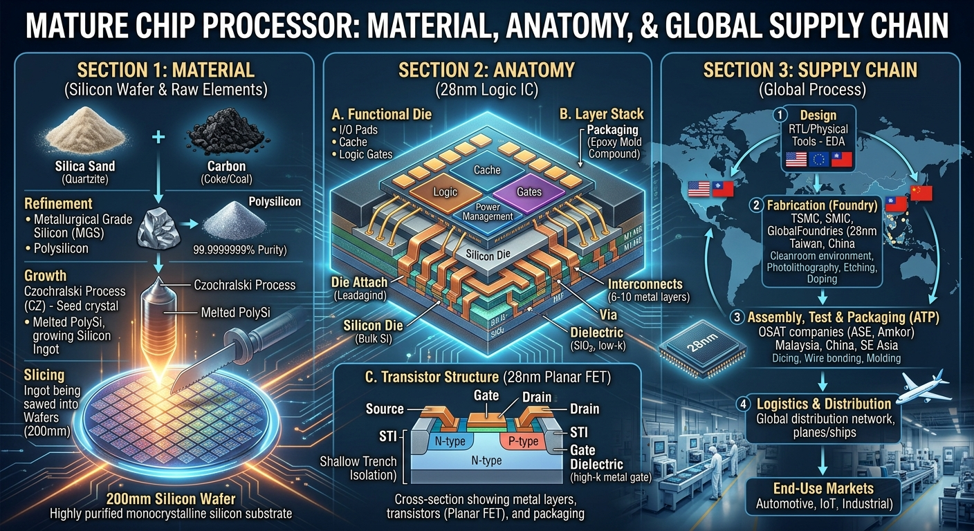
This article examines the material composition, physical anatomy, manufacturing pathway and global supply chain of mature semiconductor processors, while explaining why mature-node chips remain strategically important even as the industry develops increasingly advanced processors.
1. What Is a Semiconductor Processor?
A semiconductor processor is an integrated circuit designed to perform computational or control functions.
At its most fundamental level, the processor consists of enormous numbers of electronic devices—primarily transistors—interconnected to form functional circuits.
A transistor can act as an electrically controlled switch. By combining enormous numbers of transistors, engineers construct:
- logic gates;
- arithmetic units;
- registers;
- caches;
- control circuits;
- memory structures;
- communication interfaces;
- clock systems;
- power-management circuits; and
- complete processor architectures.
NIST defines a semiconductor as a material whose electrical conductivity can be controlled, while an integrated circuit combines many transistors into a small circuit.
The processor therefore has several different levels of identity:
Material → wafer → transistor → circuit → die → package → processor → electronic system
Understanding this hierarchy is essential to understanding the semiconductor industry.
2. What Does “Mature Chip” Mean?
The expression mature-node semiconductor does not mean an obsolete chip.
Instead, it generally refers to semiconductor manufacturing processes that are well established compared with the newest leading-edge processes.
The exact boundary changes as semiconductor technology advances. Processes that were once considered advanced eventually become established, highly optimized technologies.
Mature processes remain extremely important because many applications do not require the smallest possible transistor dimensions.
They are widely useful for:
- automobiles;
- industrial controllers;
- power-management integrated circuits;
- microcontrollers;
- sensors;
- display drivers;
- connectivity chips;
- telecommunications equipment;
- household appliances;
- medical electronics;
- embedded systems;
- security systems; and
- infrastructure equipment.
A modern vehicle, for example, can contain numerous semiconductor devices performing different functions. Some may use relatively mature manufacturing technologies because reliability, cost, high-voltage capability, analog performance or long-term availability can be more important than maximum transistor density.
Therefore, the semiconductor industry should not be understood simply as a race toward the smallest transistor.
It is better understood as a portfolio of manufacturing technologies optimized for different applications.
3. The Basic Anatomy of a Processor
A processor can be examined from several physical layers.
Layer 1: Semiconductor substrate
The foundation is normally a semiconductor wafer, commonly silicon.
Layer 2: Transistor structures
Transistors are fabricated on or within the semiconductor material.
Layer 3: Dielectric layers
Insulating materials separate conductive structures and control electrical behavior.
Layer 4: Interconnects
Extremely small metal structures connect the transistors into circuits.
Layer 5: Multiple wiring levels
Modern integrated circuits contain multiple interconnected layers rather than a single layer of wiring.
Layer 6: Protective structures
Passivation and other materials protect the circuit from environmental and mechanical damage.
Layer 7: Package
The semiconductor die is placed inside a package that provides:
- electrical connections;
- mechanical protection;
- thermal management; and
- connections to the outside world.
Layer 8: Printed circuit board
The packaged processor is mounted onto a circuit board and connected to other components.
Thus, the visible processor is only the final physical representation of a much more complicated structure.
4. Silicon: The Foundation Material
Silicon is the dominant material underlying conventional semiconductor manufacturing.
It is particularly useful because engineers can carefully control its electrical characteristics.
However, the silicon used for advanced semiconductor manufacturing is not ordinary raw material.
The manufacturing chain begins with silicon-containing resources that must eventually become extremely high-purity semiconductor material.
The material may pass through stages including:
raw material → purified silicon → polysilicon → crystal growth → ingot → wafer → polished wafer
The resulting wafer provides the foundation on which integrated circuits are fabricated.
Silicon wafers are fundamental inputs for virtually every category of semiconductor chip. NIST notes that silicon wafers are foundational to semiconductor ecosystems, including leading-edge, mature-node and memory devices.
5. The Silicon Wafer
A wafer is a thin, highly polished circular disk of semiconductor material.
A single wafer can contain many individual integrated circuits.
The basic concept is:
One large wafer → many identical chip dies
Manufacturing many devices simultaneously is one of the principal reasons semiconductor manufacturing can achieve enormous economies of scale.
The wafer must have extremely controlled:
- thickness;
- flatness;
- surface quality;
- crystal structure;
- chemical purity;
- electrical characteristics; and
- defect density.
Even tiny defects can affect semiconductor yield.
The wafer therefore represents a major technological achievement before transistor fabrication even begins.
6. Dopants and Semiconductor Electrical Properties
Pure silicon does not provide all the electrical characteristics required for practical semiconductor circuits.
Manufacturers therefore introduce controlled quantities of other elements.
This process is called doping.
Common dopant elements include:
- boron;
- phosphorus;
- arsenic; and
- other carefully controlled materials depending on the semiconductor technology.
Doping modifies the electrical properties of semiconductor regions.
The objective is not simply to add material. The concentration, location and distribution must be precisely controlled.
The result is the creation of different semiconductor regions that allow engineers to construct transistor structures.
7. Important Materials Used in Chip Manufacturing
The semiconductor industry uses hundreds of specialized materials and chemical inputs.
The Semiconductor Industry Association identifies materials such as:
- polysilicon;
- bare silicon wafers;
- epitaxial wafers;
- photomasks;
- photoresist chemicals;
- wet-processing chemicals;
- specialty gases;
- chemical-mechanical-planarization slurries;
- substrates;
- leadframes;
- encapsulation materials;
- bonding wires; and
- die-attach materials.
This demonstrates an important point:
A processor is not made from silicon alone.
Silicon is the central substrate, but the manufacturing process requires an extensive ecosystem of chemicals, metals, polymers, gases, ceramics and other engineered materials.
8. Photoresist: The Temporary Patterning Material
One of the most important materials in semiconductor manufacturing is photoresist.
Photoresist is a light-sensitive material used during lithography.
The basic concept is:
wafer → photoresist → exposure → development → patterned surface
The purpose is to transfer patterns representing parts of the integrated circuit onto the wafer.
Different photoresist systems are designed for different manufacturing technologies.
The material must exhibit highly controlled characteristics including:
- sensitivity;
- resolution;
- uniformity;
- adhesion;
- chemical resistance; and
- pattern fidelity.
Photoresist is therefore an example of a material whose performance directly influences the manufacturing process.
9. Photomasks
Photomasks are another critical component.
A photomask contains patterns used during lithography.
The manufacturing process uses the mask as part of the optical pattern-transfer system.
At a simplified level:
chip design → mask data → photomask → lithography → wafer pattern
Complex processors require extremely sophisticated pattern information.
Consequently, semiconductor manufacturing connects computer engineering and software directly with materials science and optical engineering.
10. Specialty Gases
Semiconductor fabrication requires highly controlled gases.
These gases can be used for:
- deposition;
- etching;
- cleaning;
- chamber processing;
- doping;
- plasma generation; and
- other manufacturing processes.
The purity requirements are extremely demanding.
A contaminant that would be insignificant in an ordinary industrial environment can become a serious manufacturing problem when working at microscopic or nanoscale dimensions.
This is why semiconductor fabs require elaborate systems for:
- gas purification;
- storage;
- delivery;
- monitoring;
- filtration; and
- contamination control.
11. Wet Chemicals
Wet chemicals are used for processes including:
- cleaning;
- surface preparation;
- etching;
- stripping;
- developing;
- removing unwanted materials; and
- preparing surfaces for subsequent manufacturing steps.
The semiconductor industry therefore depends heavily on chemical manufacturing.
The quality requirement extends beyond the chemical itself to:
- packaging;
- transportation;
- storage;
- delivery systems;
- filtration; and
- contamination monitoring.
A semiconductor factory is consequently also a highly sophisticated chemical-processing environment.
12. Metals Inside a Processor
Processors contain multiple conductive materials.
Copper is particularly important for electrical interconnections in many semiconductor technologies.
Other materials can also appear in different process generations and structures, including:
- aluminum;
- tungsten;
- cobalt;
- titanium;
- tantalum;
- nickel;
- gold;
- silver; and
- other specialized metals or compounds.
The exact material selection depends on the semiconductor process.
Metals can be used for:
- transistor contacts;
- interconnects;
- barriers;
- plugs;
- package connections;
- heat-transfer structures; and
- other functions.
The semiconductor industry therefore intersects strongly with global mining and refined-material supply chains.
SIA notes that semiconductor manufacturing can require silicon, gallium, germanium and other materials including palladium, tungsten, arsenic, iridium, titanium, copper and cobalt.
13. Dielectric and Insulating Materials
Not every part of a processor conducts electricity.
Insulators are equally important.
Dielectric materials separate conductive structures and help control electrical behavior.
They can be used in:
- transistor gate structures;
- isolation regions;
- interconnect layers;
- packaging;
- passivation;
- advanced substrates.
As semiconductor dimensions shrink, the properties of insulating materials become increasingly important.
Engineers must control:
- dielectric constant;
- leakage;
- mechanical stress;
- thermal behavior;
- chemical compatibility; and
- reliability.
14. Chemical Mechanical Planarization
Semiconductor manufacturing repeatedly creates new layers on the wafer.
Those layers must often be made extremely flat.
Chemical mechanical planarization (CMP) combines chemical action and mechanical polishing.
The process removes material while producing a controlled surface.
CMP requires:
- polishing pads;
- chemical slurries;
- ultrapure water;
- process control;
- precision equipment; and
- metrology.
Flatness is crucial because subsequent lithography and deposition processes depend on accurately controlled surfaces.
15. Lithography
Lithography is one of the central processes in semiconductor manufacturing.
It transfers circuit patterns onto the wafer.
At a simplified level:
- Prepare the wafer.
- Apply photoresist.
- Align the wafer.
- Expose the photoresist through the appropriate optical system.
- Develop the pattern.
- Etch or otherwise process the exposed areas.
- Remove the remaining resist when appropriate.
- Measure the result.
This cycle is repeated many times.
NIST describes lithography as the process used to create patterns on semiconductor wafers and identifies it as a fundamental part of chip fabrication.
16. Deposition
Deposition adds extremely thin layers of material to the wafer.
Different deposition technologies are used for different materials and applications.
Examples include:
- chemical vapor deposition;
- physical vapor deposition;
- atomic layer deposition; and
- epitaxial growth.
The objective is to create precisely controlled layers.
The challenge is extraordinary because engineers must control:
- thickness;
- composition;
- uniformity;
- stress;
- interface quality; and
- contamination.
17. Etching
Etching removes selected material.
It may be performed using chemical or plasma-based processes.
A simplified manufacturing cycle is:
deposit → pattern → etch → clean → measure
The process is repeated many times.
Modern semiconductor fabrication therefore resembles a highly controlled three-dimensional construction process in which material is continually added and removed.
18. Ion Implantation
Ion implantation is used to introduce controlled dopants into semiconductor materials.
The process allows manufacturers to modify electrical characteristics at specific locations.
The important variables include:
- dopant species;
- dose;
- energy;
- depth;
- temperature; and
- subsequent thermal processing.
This illustrates how semiconductor manufacturing combines physics with extremely precise industrial engineering.
19. Transistors: The Functional Core
After many fabrication steps, the wafer contains transistor structures.
The transistor is the fundamental switching element of conventional digital electronics.
A processor uses enormous numbers of these devices to implement computation.
Different generations of semiconductor technology have used different transistor structures.
The important evolution has included:
planar transistor → FinFET → newer gate-all-around architectures
The exact architecture depends on the manufacturing generation.
For mature processors, established transistor architectures may provide an excellent combination of:
- performance;
- reliability;
- manufacturing yield;
- cost;
- power efficiency; and
- long-term availability.
20. Interconnects: The Processor’s Internal Wiring
Transistors cannot perform useful computation unless they are connected.
Interconnect structures therefore create the processor’s internal wiring system.
The chip contains multiple wiring levels.
At a simplified conceptual level:
transistors → local connections → intermediate wiring → global wiring → external connections
These structures must transport electrical signals with controlled:
- resistance;
- capacitance;
- delay;
- electromagnetic behavior; and
- reliability.
As transistor density increases, interconnect engineering becomes increasingly important.
21. From Wafer to Individual Die
Once fabrication is complete, the wafer contains many individual circuits.
The wafer is inspected and tested before being separated into individual dies.
The process of separating the individual chips is commonly called dicing.
The sequence becomes:
fabricated wafer → inspection → electrical testing → dicing → individual dies
NIST describes the manufacturing sequence in which multiple integrated circuits are produced on a wafer before the wafer is diced into individual pieces.
22. Semiconductor Packaging
The bare die is not normally placed directly into a consumer product.
It needs a package.
Packaging provides:
- mechanical protection;
- electrical connections;
- thermal pathways;
- environmental protection; and
- physical integration with the circuit board.
Traditional packages include various leaded and surface-mount structures, while modern processors increasingly use sophisticated package technologies.
Packaging has become an important part of processor performance rather than merely a protective shell.
23. Advanced Packaging
As transistor scaling becomes more difficult, semiconductor companies increasingly use packaging innovation to improve system performance.
Advanced packaging can integrate:
- multiple dies;
- memory;
- logic;
- chiplets;
- high-density interconnects;
- advanced substrates; and
- specialized thermal structures.
This creates a new paradigm:
Performance improvement = transistor scaling + architecture + packaging + memory + interconnect technology
NIST research highlights the importance of polymer-based materials, substrates, underfills and other packaging materials for advanced semiconductor packaging.
24. The Material Anatomy of a Packaged Processor
A simplified packaged processor can therefore be viewed as a hierarchy:
Semiconductor core
- silicon die;
- transistor structures;
- dielectric layers;
- metal interconnects.
Die protection
- passivation;
- protective coatings.
Package
- substrate;
- package body;
- electrical contacts;
- bonding structures.
Thermal system
- heat spreader;
- thermal interface material;
- heatsink or other cooling arrangement.
System connection
- motherboard;
- power delivery;
- memory;
- communication interfaces.
The processor is therefore a multimaterial engineered system.
25. The Semiconductor Supply Chain
The supply chain can be represented approximately as:
Raw materials
↓
Purification and refining
↓
Specialty chemicals and materials
↓
Silicon wafer production
↓
Chip design and IP
↓
EDA software
↓
Photomasks
↓
Semiconductor manufacturing equipment
↓
Wafer fabrication
↓
Testing
↓
Dicing
↓
Assembly and packaging
↓
Final testing
↓
Electronics manufacturer
↓
Computer, vehicle, phone, industrial system or other product
This chain involves companies and facilities distributed across multiple countries.
26. Semiconductor Design
Before manufacturing begins, engineers design the integrated circuit.
The design process involves:
- architecture;
- logic design;
- verification;
- physical design;
- timing analysis;
- power analysis;
- security engineering;
- simulation; and
- manufacturing-rule compliance.
Electronic Design Automation, or EDA, provides software tools that make this possible.
The design is ultimately transformed into the physical patterns required for semiconductor manufacturing.
This creates a bridge between:
software → mathematics → circuit design → physical manufacturing
27. Semiconductor Manufacturing Equipment
Chip fabrication requires hundreds of specialized tools and systems.
These include equipment for:
- lithography;
- deposition;
- etching;
- cleaning;
- implantation;
- wafer handling;
- inspection;
- metrology;
- packaging; and
- testing.
SIA notes that semiconductor manufacturing equipment spans many specialized categories and can incorporate highly sophisticated subsystems such as optics, lasers, mechatronics and control electronics.
A semiconductor fab is therefore not simply a factory containing a few large machines.
It is a coordinated ecosystem of highly specialized equipment.
28. Metrology: Measuring the Invisible
Semiconductor manufacturing cannot depend only on manufacturing.
It must constantly measure the result.
Metrology provides measurements of:
- dimensions;
- film thickness;
- alignment;
- surface quality;
- defects;
- electrical properties;
- material composition;
- temperature;
- pressure; and
- process stability.
At microscopic dimensions, manufacturing and measurement become inseparable.
The basic industrial philosophy is:
make → measure → compare → correct → repeat
This feedback loop is essential for high semiconductor yields.
29. Cleanrooms
Semiconductor manufacturing takes place in highly controlled environments.
Particles can contaminate wafers and reduce yield.
Therefore, fabs control:
- airborne particles;
- temperature;
- humidity;
- vibration;
- chemical contamination;
- electromagnetic conditions;
- air pressure; and
- material movement.
Workers, equipment and materials are carefully managed.
The cleanroom is therefore part of the manufacturing technology itself.
30. Water and Environmental Infrastructure
Semiconductor fabs also require enormous supporting infrastructure.
Important systems include:
- ultrapure water;
- wastewater treatment;
- industrial gases;
- chemical distribution;
- electrical power;
- cooling systems;
- vacuum systems;
- air-handling systems;
- waste management; and
- emergency systems.
A modern semiconductor facility is consequently comparable to a combination of:
factory + laboratory + chemical plant + computer-controlled production system + precision cleanroom
31. Why the Supply Chain Is So Specialized
No single company normally produces every component required for a modern semiconductor.
One organization may specialize in:
- processor architecture;
another in:
- EDA software;
another in:
- lithography equipment;
another in:
- wafer manufacturing;
another in:
- specialty chemicals;
another in:
- packaging;
and another in:
- final electronics assembly.
This specialization creates efficiency and technological expertise.
But it also creates dependency.
NIST emphasizes that semiconductor supply chains involve thousands of suppliers and can contain multiple layers of suppliers beyond the direct relationships visible to chip manufacturers.
32. Geographic Concentration
The global semiconductor industry contains important geographic concentrations.
Different regions have developed strengths in:
- semiconductor design;
- manufacturing;
- memory;
- foundry services;
- equipment;
- materials;
- packaging;
- testing; and
- electronics assembly.
For example, silicon-wafer production is heavily concentrated in East Asia. NIST notes that approximately 90% of silicon wafers are sourced from East Asia and that a small number of major companies manage much of the global market.
This concentration creates efficiency but also creates strategic vulnerability.
33. Raw Materials and Mining
The semiconductor supply chain ultimately reaches the mining sector.
Materials can originate from:
- silicon resources;
- metal ores;
- mineral concentrates;
- natural gas;
- industrial chemicals;
- rare or specialized mineral resources.
However, mining alone is not sufficient.
A semiconductor material may need to pass through:
mining → refining → purification → chemical conversion → semiconductor-grade processing → delivery
The semiconductor industry therefore depends on a much larger industrial ecosystem than the fab itself.
34. Why Purity Matters
Ordinary industrial materials can tolerate impurities that semiconductor manufacturing cannot.
A semiconductor manufacturing material may need exceptionally high purity because contaminants can affect:
- transistor performance;
- electrical leakage;
- defects;
- yield;
- reliability;
- wafer uniformity.
Consequently, semiconductor-grade materials often require sophisticated purification and analytical testing.
This is one reason semiconductor manufacturing is difficult to reproduce quickly in a new location.
Building a fab is not enough.
A reliable local supplier ecosystem must also exist.
35. Mature Chips and Supply-Chain Security
Mature semiconductor technologies are sometimes overlooked because public attention focuses heavily on the newest processor generations.
Yet mature chips can be critical to:
- transportation;
- power systems;
- telecommunications;
- industrial automation;
- medical equipment;
- consumer electronics;
- defense-related infrastructure; and
- everyday appliances.
A shortage of mature chips can therefore disrupt entire industries.
Supply-chain resilience requires attention to both advanced and mature semiconductor manufacturing.
36. The Role of Testing
A chip is not finished when fabrication ends.
Testing determines whether it performs according to specification.
Testing can occur at several stages:
- wafer-level testing;
- die testing;
- package testing;
- final electrical testing;
- reliability testing.
Manufacturers examine characteristics such as:
- functionality;
- voltage;
- frequency;
- power consumption;
- temperature behavior;
- electrical leakage;
- reliability; and
- manufacturing defects.
Only devices that meet appropriate specifications proceed through the supply chain.
37. Yield: One of the Most Important Concepts
Yield represents the proportion of manufactured devices that successfully meet required specifications.
Yield is crucial to semiconductor economics.
Imagine a wafer containing hundreds of dies.
If a large percentage works correctly, manufacturing economics can be excellent.
If many dies fail, the cost of each usable chip increases.
Therefore:
Yield = technology + materials + equipment + process control + metrology + experience
This is one reason established mature processes can be economically powerful.
Years of optimization can produce highly predictable manufacturing performance.
38. Mature Technology Can Be Extremely Valuable
A mature process can offer several advantages:
- proven manufacturing;
- established equipment;
- qualified materials;
- mature supply chains;
- high yields;
- predictable reliability;
- lower development risk;
- long product lifetimes.
For many applications, the newest process is unnecessary.
An automotive control chip does not necessarily need the same transistor technology as a high-performance artificial-intelligence processor.
The correct semiconductor process depends on the application’s engineering requirements.
39. The Relationship Between Chip Materials and Chip Performance
Material selection influences:
electrical performance
thermal performance
manufacturing yield
reliability
cost
power consumption
frequency
device lifetime
packaging compatibility
Thus, materials science is not an isolated part of semiconductor manufacturing.
It directly influences the final processor.
40. Thermal Management
As processors perform more computation, they generate heat.
Heat must be transported away from the semiconductor die.
The thermal path can be simplified as:
transistor → die → package → thermal interface → heat spreader → heatsink/cooling system → surrounding environment
Thermal engineering is particularly important for high-performance processors.
Packaging materials must therefore satisfy not only electrical requirements but also mechanical and thermal requirements.
41. Reliability and Aging
Semiconductor devices must operate for years in many applications.
Engineers therefore study mechanisms including:
- electromigration;
- dielectric degradation;
- thermal cycling;
- mechanical stress;
- corrosion;
- material fatigue;
- package cracking;
- moisture effects.
Packaging materials are especially important because differences in thermal expansion between materials can create mechanical stress.
NIST’s recent work on advanced packaging emphasizes issues such as residual stress, moisture reliability, warpage and polymer-material behavior.
42. Semiconductor Supply-Chain Risks
The semiconductor supply chain can be affected by:
Natural disasters
Earthquakes, floods, fires and storms can interrupt production.
Energy shortages
Fabs require reliable electricity.
Water shortages
Manufacturing depends on highly controlled water systems.
Transportation disruptions
Materials and components must move across international borders.
Geopolitical tensions
Trade restrictions and export controls can affect equipment, materials and technology.
Concentration
If only a few suppliers produce a critical material, disruption can have global consequences.
Manufacturing accidents
A single facility can sometimes be an important source of a specialized input.
These risks demonstrate why semiconductor resilience is a strategic economic issue.
43. Supply-Chain Traceability
A modern semiconductor company needs to understand not only its direct suppliers but also important suppliers deeper in the chain.
The chain may look like:
Chip manufacturer
↓
Chemical supplier
↓
Chemical producer
↓
Refinery
↓
Mineral processor
↓
Mine
A disruption several levels upstream can eventually reach the chip manufacturer.
NIST has emphasized the importance of traceability and supply-chain visibility because semiconductor manufacturing contains many layers of suppliers.
44. Building a Resilient Semiconductor Ecosystem
A resilient ecosystem requires diversification.
Important strategies include:
- Multiple qualified suppliers.
- Geographic diversification.
- Strategic inventories.
- Alternative materials where technically feasible.
- Recycling and recovery.
- Improved supplier visibility.
- Domestic or regional manufacturing capacity.
- Strong metrology and quality-control systems.
- Skilled semiconductor workers.
- Research and development.
The objective is not necessarily to manufacture everything within one country.
Rather, the objective is to avoid dangerous dependence on a single point of failure.
45. Recycling and Circular Manufacturing
The semiconductor industry can also improve resource efficiency through recovery and recycling.
Potentially valuable materials include:
- metals;
- process chemicals;
- solvents;
- water;
- specialty materials.
Advanced recovery systems can reduce:
- raw-material consumption;
- waste;
- environmental impact;
- operating costs.
The challenge is that semiconductor manufacturing has extremely demanding purity requirements, so recovered materials must be processed appropriately before reuse.
46. Artificial Intelligence and Semiconductor Materials
Artificial intelligence is increasing demand for computing infrastructure.
AI processors require advanced:
- logic;
- memory;
- packaging;
- networking;
- power delivery;
- cooling.
However, AI growth also affects mature semiconductor demand.
Data centers require many supporting components beyond the main AI accelerator.
These can include:
- power-management chips;
- microcontrollers;
- network controllers;
- sensors;
- monitoring circuits;
- storage controllers;
- interface chips.
Consequently, AI represents demand across the semiconductor ecosystem rather than only for the most advanced processor.
47. The Future of Semiconductor Materials
The semiconductor industry is investigating numerous approaches to extend performance beyond conventional scaling.
These include:
- new transistor architectures;
- advanced dielectric materials;
- improved interconnect materials;
- compound semiconductors;
- advanced substrates;
- chiplets;
- three-dimensional integration;
- optical technologies;
- advanced packaging;
- improved thermal materials.
The future is therefore unlikely to depend on a single material or single technology.
Instead, progress will increasingly emerge from the combination of:
materials + transistor architecture + manufacturing + packaging + software + system architecture
48. From Mine to Microprocessor: The Complete Journey
The entire story can be summarized as follows:
1. Natural resources
Minerals and chemical feedstocks are extracted.
↓
2. Refining
Raw materials are purified.
↓
3. Semiconductor-grade materials
Highly controlled materials are produced.
↓
4. Silicon production
High-purity silicon becomes crystalline material.
↓
5. Wafer manufacturing
Silicon ingots are converted into polished wafers.
↓
6. Chip design
Engineers create the processor architecture and circuit design.
↓
7. Mask and process preparation
Design information becomes manufacturing patterns.
↓
8. Front-end fabrication
Transistors and semiconductor structures are created.
↓
9. Interconnect fabrication
Metal wiring connects the circuit.
↓
10. Metrology
The wafer is inspected and measured.
↓
11. Wafer testing
Individual circuits are evaluated.
↓
12. Dicing
Individual dies are separated.
↓
13. Packaging
The die becomes a protected electronic component.
↓
14. Final testing
The packaged processor is tested.
↓
15. Distribution
Processors move to electronics manufacturers.
↓
16. System integration
The processor becomes part of a computer, vehicle, telecommunications system, industrial machine or other product.
49. Why Semiconductor Manufacturing Is So Difficult
The fundamental challenge is not simply making a tiny transistor.
The challenge is making billions of extremely precise structures repeatedly, economically and reliably.
The industry must simultaneously control:
- physics;
- chemistry;
- materials;
- optics;
- mechanics;
- electronics;
- software;
- heat;
- contamination;
- vibration;
- electricity;
- water;
- gases;
- logistics;
- quality;
- testing;
- economics.
This is why semiconductor manufacturing is one of the world’s most sophisticated industrial activities.
50. Strategic Importance for Developing Economies
Countries seeking to strengthen their technology sectors do not necessarily need to begin by building the world’s most advanced processor fab.
A broader semiconductor ecosystem can include:
- electronics design;
- embedded software;
- PCB manufacturing;
- semiconductor testing;
- packaging;
- repair and refurbishment;
- materials research;
- equipment maintenance;
- technical education;
- industrial automation;
- power electronics;
- sensors;
- semiconductor distribution;
- research laboratories.
This creates opportunities for participation at different points of the value chain.
For countries in Africa, this broader perspective can be particularly important. A national semiconductor strategy can begin with education, electronics assembly, design capability, testing, packaging, industrial electronics and research while developing the infrastructure required for more advanced manufacturing over time.
51. South Africa and the Broader African Opportunity
South Africa possesses capabilities relevant to the wider semiconductor ecosystem, including scientific research, engineering, mining, telecommunications, electronics and advanced manufacturing.
Africa’s mineral resources also create an important connection to the global materials economy.
However, the strategic objective should not simply be to export raw minerals.
A higher-value pathway would seek to develop progressively greater capabilities:
minerals → refined materials → specialty materials → electronic components → semiconductor-related manufacturing → chip design → advanced electronics
Such development requires:
- mathematics education;
- physics;
- chemistry;
- engineering;
- computer science;
- industrial automation;
- clean manufacturing;
- reliable electricity;
- water infrastructure;
- research institutions;
- technical skills;
- investment; and
- international partnerships.
The semiconductor industry is ultimately a knowledge-intensive industrial ecosystem.
52. The Processor as a Global Industrial Product
A processor therefore represents much more than a piece of silicon.
It embodies:
geology
through mineral resources;
chemistry
through purification and processing;
materials science
through semiconductor and packaging materials;
physics
through transistor operation;
optics
through lithography;
mechanical engineering
through manufacturing equipment;
computer science
through architecture and design;
software engineering
through EDA and verification;
industrial engineering
through process control;
logistics
through global supply chains;
economics
through capital investment and yield;
and
international cooperation
through global specialization.
This makes the semiconductor one of the clearest examples of how modern civilization combines many scientific and industrial disciplines into one product.
Conclusion
The mature semiconductor processor is the result of an extraordinarily sophisticated technological chain.
Its visible form may be a small packaged component, but beneath that package lies a multilayered architecture of silicon, dopants, dielectric materials, metals, polymers, substrates and protective structures. These materials are transformed through hundreds or thousands of carefully controlled manufacturing operations.
The supply chain begins far upstream with minerals, chemicals and refined materials. It continues through silicon production, wafer manufacturing, processor design, EDA, photomasks, semiconductor equipment, fabrication, metrology, testing, packaging and logistics before finally reaching the electronic system.
Mature semiconductor technology deserves particular attention because it is not synonymous with obsolete technology. Established manufacturing processes remain essential to automobiles, telecommunications, industrial machinery, consumer electronics, infrastructure and many other sectors.
The semiconductor industry is therefore best understood as a global technological ecosystem rather than a single factory or product.
Its future will depend not only on smaller transistors, but also on better materials, advanced packaging, chiplet architectures, improved manufacturing, stronger supply-chain resilience, artificial intelligence, thermal engineering, metrology and the development of skilled scientific and engineering workforces.
Ultimately, the journey from raw material to processor demonstrates one of the central achievements of modern technology: the ability to transform ordinary elements of the physical world into extraordinarily complex machines capable of controlling information, computation and communication on a global scale.
Selected References
- NIST, Semiconductor Glossary and semiconductor manufacturing resources.
- NIST, Vision for Success: Facilities for Semiconductor Materials and Manufacturing Equipment.
- Semiconductor Industry Association, 2025 State of the U.S. Semiconductor Industry.
- Semiconductor Industry Association, semiconductor supply-chain and materials information.
- NIST, research on advanced semiconductor packaging materials and metrology.



Be First to Comment