
Abstract
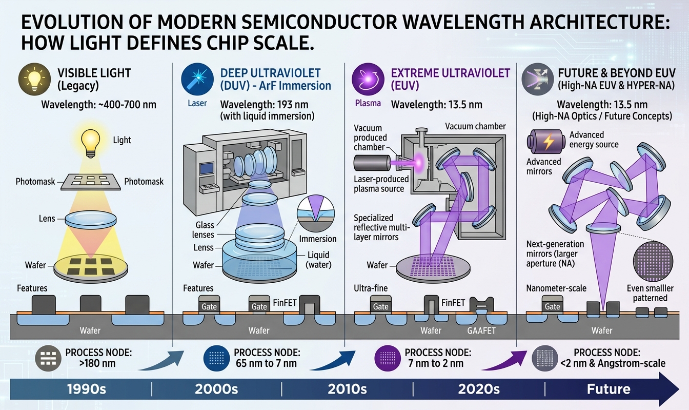
Modern semiconductor manufacturing is fundamentally an information-transfer process using light. A chip designer creates an electronic circuit, but the manufacturing system must physically transfer that circuit pattern onto a silicon wafer with extraordinary precision.
The central technology enabling this is photolithography—the controlled use of electromagnetic radiation to define microscopic structures in semiconductor materials.
The history of semiconductor lithography can therefore be understood as a progression toward:
shorter wavelength → higher numerical aperture → better pattern control → smaller printable features → greater transistor density.
Modern leading-edge manufacturing uses several wavelength generations simultaneously. DUV systems commonly use 365 nm, 248 nm and 193 nm radiation, while EUV uses 13.5 nm radiation. ASML
1. The Fundamental Idea
A semiconductor wafer is essentially a highly engineered platform on which billions of microscopic structures are constructed.
The manufacturing problem is:
How can we take a computer-designed circuit pattern and reproduce it accurately on silicon at nanometer-scale dimensions?
The answer is lithography.
A simplified chain is:
Computer circuit design
↓
Photomask/reticle
↓
Light source
↓
Optical system
↓
Photoresist
↓
Silicon wafer
↓
Developing
↓
Etching/deposition/implantation
↓
Transistor structures
↓
Interconnects
↓
Integrated circuit
Lithography is therefore analogous to a microscopic printing system—but vastly more precise.
2. What Does “Wavelength” Mean?
Wavelength, represented by λ (lambda), is the distance between corresponding points of a wave.
For electromagnetic radiation:\[ c = f\lambda \]
where:
- \(c\) = speed of light
- \(f\) = frequency
- \(\lambda\) = wavelength
Therefore:\[ f = \frac{c}{\lambda} \]
As wavelength decreases, frequency increases.
For example:
| Lithography radiation | Wavelength |
|---|---|
| Mercury i-line | 365 nm |
| KrF DUV | 248 nm |
| ArF DUV | 193 nm |
| EUV | 13.5 nm |
The enormous reduction from 193 nm to 13.5 nm is one of the most important transitions in modern semiconductor manufacturing. EUV’s wavelength is about 14 times shorter than 193 nm DUV. ASML
3. Why Shorter Wavelength Helps
A useful simplified analogy is a pencil.
A thick pencil cannot easily draw extremely fine lines.
A very fine writing instrument can reproduce much smaller details.
Light behaves differently from a mechanical pencil, but the analogy captures the fundamental manufacturing challenge:
shorter wavelength allows optical systems to resolve finer spatial details.
The fundamental relationship is represented by the Rayleigh criterion:\[ CD = k_1\frac{\lambda}{NA} \]
where:
- \(CD\) = critical dimension
- \(k_1\) = process factor
- \(\lambda\) = wavelength
- \(NA\) = numerical aperture
Thus:\[ CD \propto \frac{\lambda}{NA} \]
This means manufacturers can improve resolution primarily by:
- decreasing wavelength,
- increasing numerical aperture,
- improving the process factor \(k_1\),
- improving computational and process control.
ASML describes this same Rayleigh relationship as a fundamental basis for lithographic resolution. ASML
4. The Semiconductor Wavelength Evolution
The development can be viewed as a technological ladder.
Generation 1 — Mercury lamps
Early lithography used mercury-vapor lamps.
Important wavelengths included:
436 nm → 365 nm
The 365 nm wavelength became known as i-line lithography.
It allowed progressively smaller features compared with earlier visible-light systems. ASML
Generation 2 — KrF
The industry moved toward excimer lasers.
Krypton fluoride (KrF) produces:\[ \lambda = 248\,nm \]
This was a major reduction from 365 nm.
Modern KrF systems can produce substantially smaller features than the earlier i-line generation. ASML
Generation 3 — ArF
The next major transition was:
Argon fluoride (ArF)\[ \lambda = 193\,nm \]
193 nm became extraordinarily important because it remained useful for advanced manufacturing far beyond what might initially have been expected.
The introduction of immersion lithography allowed 193 nm systems to achieve still higher numerical aperture. ASML
5. The Brilliant Idea of Immersion Lithography
One of the most important developments was placing a very thin layer of water between the final optical element and the wafer.
Why?
Because numerical aperture depends partly on refractive index.
Simplified:\[ NA=n\sin\theta \]
where \(n\) is the refractive index of the medium.
Water has a higher refractive index than air.
Therefore:
air
→ lower effective NA
water
→ higher effective NA
Modern ArF immersion systems have reached approximately:\[ NA=1.35 \]
according to ASML. ASML
This allowed 193 nm technology to continue producing increasingly small structures without immediately requiring a completely new wavelength.
6. Why 193 nm Was Not Enough Forever
The industry eventually reached physical and economic limits.
Instead of continuously trying to extract more resolution from 193 nm radiation, semiconductor manufacturers needed another fundamental wavelength transition.
That transition was:
13.5 nm EUV
EUV means:
Extreme Ultraviolet.
The wavelength is:\[ \lambda = 13.5\,nm \]
This is dramatically shorter than 193 nm.
The difference is:\[ \frac{193}{13.5}\approx14.3 \]
So EUV has a wavelength approximately 14 times shorter than 193 nm DUV. ASML
7. The Architecture of an EUV System
An EUV lithography machine is not simply a more powerful ultraviolet projector.
It requires an entirely different architecture.
A simplified architecture is:
HIGH-POWER LASER
       │
       ▼
TIN DROPLETS
       │
       ▼
TIN PLASMA
       │
       ▼
13.5 nm EUV LIGHT
       │
       ▼
COLLECTOR MIRROR
       │
       ▼
MULTILAYER MIRRORS
       │
       ▼
EUV RETICLE
       │
       ▼
PROJECTION MIRRORS
       │
       ▼
PHOTORESIST
       │
       ▼
SILICON WAFER
The system operates in vacuum because EUV radiation is strongly absorbed by air and many ordinary materials. ASML
8. How the 13.5 nm Light Is Actually Created
This is one of the most remarkable aspects of semiconductor engineering.
A conventional laser cannot simply generate the required EUV output directly in the same way as a 193 nm excimer laser system.
Instead, EUV systems use a laser-produced plasma (LPP) architecture.
Tiny droplets of molten tin are generated and accelerated through the source.
A laser interacts with the tin droplet.
The process approximately follows:
tin droplet
→ laser pulse
→ droplet deformation
→ intense laser interaction
→ vaporization/ionization
→ extremely hot plasma
→ EUV radiation
→ collection
→ optical system
ASML describes its EUV source as using laser pulses on tin droplets, with the process occurring tens of thousands of times per second in modern systems. ASML
9. Why Tin?
Tin is particularly useful because its highly ionized plasma can emit radiation strongly around the desired 13.5 nm wavelength.
The objective is not simply:
“Make light.”
The objective is:
Generate enormous quantities of precisely useful 13.5 nm photons with sufficient stability and power for industrial semiconductor production.
That distinction is extremely important.
10. Why EUV Needs Mirrors Instead of Lenses
This is another fundamental architectural difference.
In ordinary optical systems, lenses transmit and refract light.
But EUV radiation is absorbed strongly by ordinary materials.
Therefore, conventional glass lenses cannot simply be used.
Instead:
DUV
uses primarily:
precision lenses
while
EUV
uses:
precision multilayer mirrors.
ASML describes EUV optical systems as using multilayer mirrors, with individual mirrors containing more than 100 carefully engineered layers. ASML
11. EUV Mirror Architecture
An EUV mirror is not an ordinary mirror.
It is effectively a nanoscale engineered interference structure.
It contains alternating layers of materials designed so that EUV radiation is reflected through constructive interference.
Conceptually:
Incoming EUV
     ↓
────────────────
Layer A
────────────────
Layer B
────────────────
Layer A
────────────────
Layer B
────────────────
Layer A
────────────────
Layer B
────────────────
      ↓
Reflected EUV
The thickness and uniformity of these layers must be extraordinarily precise.
The mirror surface itself must also be exceptionally smooth. ASML
12. The Reticle
The reticle is the pattern carrier.
It contains the geometric information required to create particular structures on the wafer.
In conventional DUV lithography, the mask operates primarily through transmission.
In EUV, the reticle is reflective.
Therefore:
EUV light
   ↓
Reflective reticle
   ↓
Patterned reflection
   ↓
Projection optics
   ↓
Wafer
The optical system reduces the reticle pattern before projecting it onto the wafer. ASML describes a 4× reduction in its EUV optical systems. ASML
13. Photoresist: The Light-Sensitive Material
Before exposure, the wafer receives a very thin layer of photoresist.
Think of photoresist as a molecular recording medium.
The process is approximately:
Silicon wafer
      ↓
Resist coating
      ↓
EUV/DUV exposure
      ↓
Chemical transformation
      ↓
Development
      ↓
Pattern revealed
Different photoresist chemistries behave differently when illuminated.
For positive resist, exposed regions become more soluble in the developer.
For negative resist, exposure can make regions less soluble. ASML
14. From Light Pattern to Physical Transistor
This is where lithography becomes semiconductor manufacturing.
Lithography itself doesn’t create the complete transistor.
Instead, it creates a temporary physical pattern.
That pattern then controls subsequent processes.
For example:
Lithography
     ↓
Pattern
     ↓
Etching
     ↓
Material removed
     ↓
Deposition
     ↓
New material added
     ↓
Ion implantation / doping
     ↓
Electrical properties modified
These processes are repeated many times.
15. A Modern Chip Is a Multilayer Structure
A modern processor isn’t simply one patterned layer.
It can contain a very large number of patterned layers.
At the transistor level:
Gate
 │
 ├── dielectric
 │
 ├── semiconductor
 │
 └── source/drain
Above the transistor layer are increasingly complex interconnect structures.
Conceptually:
Metal interconnect
════════════════════
Metal interconnect
════════════════════
Via structures
│ │ │ │ │ │
Transistors
▐▐▐▐▐▐▐▐
Silicon substrate
════════════════════
Every layer requires extremely accurate alignment with the layers beneath it.
16. Overlay: The Hidden Problem
Suppose you successfully print one layer.
Now you must print another layer directly above it.
If the second layer moves by even a tiny amount, electrical structures may not connect correctly.
This is called overlay accuracy.
Therefore modern lithography requires simultaneous control of:
- wavelength,
- focus,
- stage position,
- alignment,
- temperature,
- vibration,
- optics,
- wafer deformation,
- resist behavior,
- pattern distortion.
The machine is therefore much more than an optical projector.
It is an enormous precision control system.
17. The Wafer Stage
The wafer must move with extraordinary precision.
During exposure, the stage controls the position of the wafer relative to the projected image.
Modern EUV systems use sophisticated positioning and measurement systems.
ASML reports that its wafer stage can position the wafer to extremely small tolerances while continuously measuring and correcting its position. ASML
Conceptually:
                 Measurement
                     ↓
              ┌─────────────┐
              │ Control CPU  │
              └──────┬──────┘
                     ↓
Laser ──→ Optics ──→ Wafer
                     ↑
                 Stage
                     ↑
                 Sensors
This is a closed-loop control architecture.
18. Computational Lithography
Modern lithography is increasingly computational.
The physical pattern created on the wafer is not simply identical to the computer drawing.
Light diffraction, resist chemistry, optics and other physical effects distort the image.
Therefore sophisticated mathematical models predict these effects.
The design can then be deliberately modified before exposure.
Conceptually:
Original circuit
       ↓
Optical simulation
       ↓
Distortion prediction
       ↓
Pattern correction
       ↓
Reticle
       ↓
Exposure
       ↓
Wafer
This is one reason semiconductor manufacturing increasingly combines:
physics + optics + chemistry + mathematics + computer science + control engineering + artificial intelligence/data analysis.
ASML identifies computational lithography as an important part of its lithography portfolio. ASML
19. Why “2 nm” Does Not Mean 2 nm Wavelength
This is extremely important.
A modern semiconductor process described as:
7 nm
5 nm
3 nm
2 nm
does not mean the lithography wavelength is 7, 5, 3 or 2 nm.
For example:\[ \text{2-nm-class process} \neq 2\,nm\ lithography\ wavelength \]
Leading-edge EUV lithography uses 13.5 nm light, including for advanced nodes. ASML
The “node” designation refers to a semiconductor manufacturing generation and associated dimensions/density/performance characteristics—not simply the wavelength of the lithography light.
This distinction prevents one of the most common misunderstandings about modern semiconductor technology.
20. High-NA EUV
The next major architectural improvement is not primarily another dramatic wavelength reduction.
Instead, the industry is increasing:\[ NA \]
from approximately:\[ 0.33 \]
to:\[ 0.55 \]
in High-NA EUV systems.
The Rayleigh relationship explains why:\[ CD = k_1\frac{\lambda}{NA} \]
If wavelength remains approximately:\[ 13.5\,nm \]
but NA increases substantially, the theoretical resolution improves.
ASML’s High-NA EUV platform uses 0.55 NA and is designed for future advanced logic and memory manufacturing. ASML
21. The Modern Wavelength Architecture
We can therefore visualize semiconductor lithography as an evolutionary architecture:
436 nm
  │
  ▼
365 nm
  │
  ▼
248 nm
  │
  ▼
193 nm
  │
  ├── Dry DUV
  │
  └── Immersion DUV
          │
          ▼
      13.5 nm EUV
          │
          ▼
      High-NA EUV
But the industry does not simply throw away the previous technology.
Instead:
Advanced chips
      │
      ├── EUV
      │
      ├── ArF immersion
      │
      ├── ArF dry
      │
      ├── KrF
      │
      └── i-line
Different layers and different types of chips require different lithography technologies.
ASML explicitly notes that EUV and DUV systems operate in parallel, with DUV continuing to print many chip layers. ASML
22. Why Semiconductor Manufacturing Is Really a “Wavelength Architecture”
The phrase can be understood at several levels.
Level 1 — Electromagnetic physics
\[ \lambda,\ f,\ c \]
determine the fundamental properties of the radiation.
Level 2 — Optical architecture
\[ \lambda + NA \]
determine achievable optical resolution.
Level 3 — Lithography
The optical system transfers patterns onto photoresist.
Level 4 — Materials
Resist, silicon, dielectrics, metals and other materials transform the optical pattern into physical structures.
Level 5 — Electronics
Those structures become:
- transistors,
- capacitors,
- resistors,
- contacts,
- vias,
- interconnects.
Level 6 — Computing
Billions of these structures form:
- CPUs,
- GPUs,
- AI accelerators,
- memory,
- communication processors,
- sensors.
Thus:\[ \boxed{ \text{Electromagnetic waves} \rightarrow \text{patterns} \rightarrow \text{materials} \rightarrow \text{transistors} \rightarrow \text{logic} \rightarrow \text{computation} } \]
23. The Deeper Scientific Picture
The remarkable thing about modern semiconductor manufacturing is that macroscopic engineering controls microscopic quantum-scale structures.
A modern lithography system combines:
Physics
Electromagnetism, diffraction, plasma physics and quantum effects.
Optics
Lenses, mirrors, numerical aperture and interference.
Chemistry
Photoresists, developers, deposition and etching.
Materials science
Silicon, metals, dielectrics and multilayer optical materials.
Mechanical engineering
Precision stages and vibration isolation.
Mechatronics
Thousands of actuators and sensors.
Computer science
Pattern computation and process control.
Mathematics
Fourier optics, diffraction theory, optimization and statistical process control.
Semiconductor engineering
Transistor and interconnect architecture.
This makes modern lithography one of the most interdisciplinary engineering systems ever developed.
24. The Complete Modern Semiconductor Patterning Loop
A useful final architecture is:
                 CHIP DESIGN
                     │
                     ▼
              Circuit geometry
                     │
                     ▼
             Computational
               lithography
                     │
                     ▼
                  Reticle
                     │
                     ▼
          ┌────────────────────┐
          │   LIGHT SOURCE     │
          │                    │
          │ DUV → 193/248 nm   │
          │ EUV → 13.5 nm      │
          └─────────┬──────────┘
                    │
                    ▼
                OPTICS
                    │
             ┌──────┴──────┐
             │             │
          DUV lenses    EUV mirrors
             │             │
             └──────┬──────┘
                    ▼
                  WAFER
                    │
                    ▼
                PHOTORESIST
                    │
                    ▼
                DEVELOPMENT
                    │
                    ▼
                  ETCH
                    │
                    ▼
               DEPOSITION
                    │
                    ▼
             DOPING / IMPLANT
                    │
                    ▼
              TRANSISTOR
                STRUCTURE
                    │
                    ▼
             INTERCONNECTS
                    │
                    ▼
             COMPLETE CHIP
25. The Central Equation
The entire technological race can be summarized initially by:\[ \boxed{CD=k_1\frac{\lambda}{NA}} \]
This equation explains much of semiconductor lithography’s history.
When engineers could no longer easily improve one variable, they attacked another.
First major strategy:
Reduce:\[ \lambda \]
Second strategy:
Increase:\[ NA \]
Third strategy:
Reduce:\[ k_1 \]
through increasingly sophisticated process technology and computational techniques.
Therefore semiconductor scaling is not simply:
“Make the light wavelength smaller.”
It is:
Optimize an entire physical information-transfer system.
26. The Most Important Concept to Remember
The modern semiconductor industry is not actually manufacturing transistors with light alone.
Instead, light is the extremely precise information carrier that tells the wafer where material should eventually be removed, added, modified or electrically connected.
The deeper chain is:\[ \boxed{ \text{Information} \rightarrow \text{Optical pattern} \rightarrow \text{Chemical pattern} \rightarrow \text{Material structure} \rightarrow \text{Electrical structure} \rightarrow \text{Computer} } \]
That is the real architecture of semiconductor lithography.
And the progression from 365 nm → 248 nm → 193 nm → 13.5 nm → High-NA EUV represents a remarkable history of engineering electromagnetic waves into an industrial tool capable of constructing incredibly dense electronic systems. ASML
Key reference points
- 193 nm ArF DUV: remains a major lithography technology, particularly with immersion.
- 13.5 nm EUV: enables the most intricate layers of leading-edge chips.
- 0.33 NA EUV: established EUV architecture.
- 0.55 NA High-NA EUV: increases resolution without requiring a new wavelength.
- 2 nm-class nodes: are manufacturing generations; they should not be confused with a 2 nm lithography wavelength. ASML




Be First to Comment