
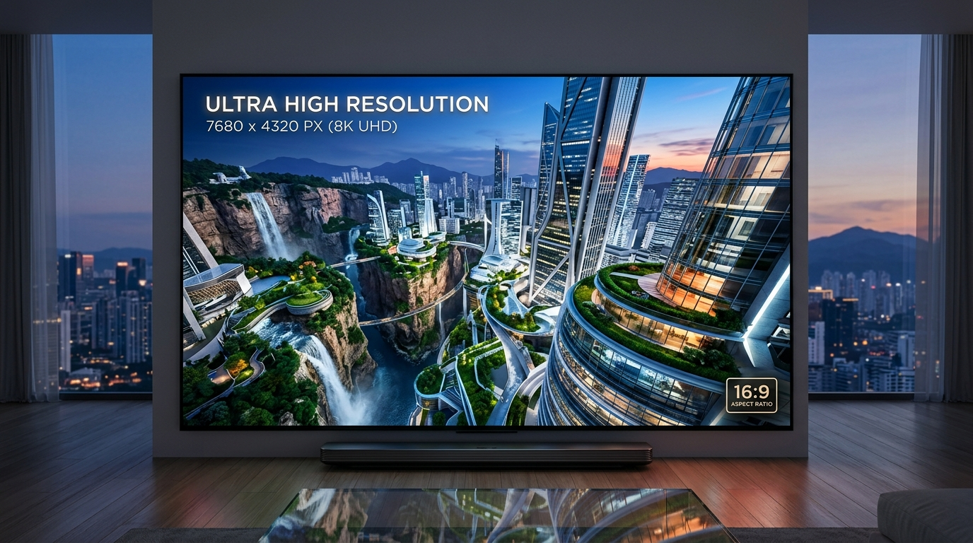
Thesis on Pixels, 4K, 8K, 16K, OLED, MicroLED, and Visual Computing
Abstract
Modern display technology is the result of a convergence between physics, semiconductor engineering, materials science, optical design, computer architecture, and manufacturing. Screen resolution has progressed from standard-definition television to Full HD, 4K Ultra HD, 8K Ultra HD, and emerging 16K systems. This progression represents a substantial increase in the number of independently controlled picture elements, or pixels, that can be reproduced on a screen.
However, resolution alone does not determine visual quality. A display is a complete system consisting of a video source, processing electronics, a display interface, a semiconductor backplane, light-emitting or light-modulating materials, optical layers, and a human observer. The practical value of higher resolution depends on pixel density, viewing distance, brightness, contrast, colour accuracy, refresh rate, response time, content quality, and manufacturing cost.
This thesis examines the mathematical foundations of resolution, the physics of light emission and modulation, the architecture of active-matrix displays, and the manufacturing processes used in OLED and MicroLED technologies. It also investigates the data and bandwidth requirements of high-resolution video, the role of artificial intelligence in image processing, and the technological challenges associated with 16K and future displays.
The central argument is that the future of display technology is not simply a race toward more pixels. It is the development of more efficient, more precise, more durable, and more intelligent visual systems.
Keywords: Screen resolution, pixels, 4K, 8K, 16K, OLED, MicroLED, semiconductor, TFT, CMOS, HDR, pixel density, display manufacturing, visual computing.
Chapter 1: Introduction
1.1 Background
Screens have become one of the principal interfaces between humans and digital information. Television, smartphones, computers, medical instruments, vehicles, scientific equipment, and industrial control systems all depend on displays to convert electronic information into visible images.
The development of display technology has followed several major transitions:
- Cathode-ray tube displays
- Liquid-crystal displays
- High-definition digital displays
- OLED and advanced LCD systems
- MicroLED and other emerging self-emissive technologies
At the same time, resolution has increased from millions to tens of millions of pixels, with experimental and specialised systems reaching more than one hundred million pixels.
A modern display is therefore not merely a screen. It is a large-scale electronic computing system whose output is light.
1.2 Research Problem
The public discussion of modern screens often reduces technological progress to statements such as:
“8K is better than 4K.”
or:
“16K is the latest resolution.”
These statements are incomplete. They do not explain:
- What a pixel physically is
- How a semiconductor controls a pixel
- How light is produced
- How millions of pixels are manufactured
- Why higher resolution requires more data
- Why a higher-resolution display may not always look better
- Why OLED and MicroLED have different engineering advantages
- Why 16K is not automatically the next mainstream television standard
The research problem is therefore:
How does modern screen resolution develop from a mathematical specification into a practical visual system, and what technological factors determine its future?
1.3 Research Aim
The aim of this thesis is to develop a comprehensive scientific and engineering understanding of modern screen resolution, from the physics of individual pixels to the architecture and manufacturing of high-resolution display systems.
1.4 Research Objectives
The study seeks to:
- Explain the mathematical meaning of screen resolution.
- Analyse the physics of pixels and light.
- Examine semiconductor backplane architecture.
- Explain OLED and MicroLED operating principles.
- Describe major manufacturing processes.
- Compare 4K, 8K, and 16K systems.
- Calculate pixel density and data requirements.
- Examine the relationship between resolution and picture quality.
- Investigate emerging display technologies.
- Identify the major challenges facing future high-resolution displays.
1.5 Research Questions
- What is screen resolution?
- How does a pixel produce or control light?
- How do semiconductor circuits address millions of pixels?
- What are the physical differences between LCD, OLED, and MicroLED?
- How are high-resolution display panels manufactured?
- Why does resolution increase data and processing requirements?
- What determines whether higher resolution is visible to the human eye?
- What are the practical advantages and limitations of 8K and 16K?
- What manufacturing challenges limit MicroLED adoption?
- What developments are likely to shape the future of display technology?
1.6 Hypotheses
H1: Higher resolution increases potential image detail, but its visible benefit depends on pixel density, viewing distance, and source quality.
H2: Semiconductor backplane architecture is a fundamental determinant of display resolution, refresh rate, brightness control, and manufacturing yield.
H3: OLED and MicroLED offer important advantages over conventional LCD architectures, but their manufacturing challenges differ.
H4: The future of display technology will combine higher resolution with improved optical performance, processing intelligence, and manufacturing efficiency.
1.7 Scope
This thesis focuses on modern flat-panel and emerging high-resolution displays. It includes:
- LCD
- OLED
- AMOLED
- QD-OLED
- Mini-LED backlit LCD
- MicroLED
- 4K, 8K, and 16K
- Pixel physics
- Semiconductor architecture
- Display manufacturing
- Video bandwidth
- AI image processing
It does not attempt to provide a complete history of every display technology or a detailed commercial ranking of current products.
Chapter 2: The Mathematical Foundations of Resolution
2.1 Definition of a Pixel
A pixel is the smallest independently addressable picture element in a digital display.
A colour pixel commonly consists of three subpixels:
- Red
- Green
- Blue
These subpixels combine different intensities of light to produce a wide range of colours.
The total number of pixels in a rectangular display is:
where:
- = total pixels
- = horizontal pixel count
- = vertical pixel count
2.2 Resolution Examples
| Resolution | Horizontal pixels | Vertical pixels | Total pixels |
|---|---|---|---|
| 720p | 1280 | 720 | 921,600 |
| 1080p | 1920 | 1080 | 2,073,600 |
| 4K UHD | 3840 | 2160 | 8,294,400 |
| 8K UHD | 7680 | 4320 | 33,177,600 |
| 16K | 15360 | 8640 | 132,710,400 |
The standard 4K and 8K UHD dimensions are widely used in modern television systems.
2.3 Resolution Ratios
The relationship between two resolutions can be calculated by dividing their total pixel counts.
4K compared with 1080p
Therefore:
4K contains four times as many pixels as Full HD.
8K compared with 4K
Therefore:
8K contains four times as many pixels as 4K.
16K compared with 4K
Therefore:
16K contains sixteen times as many pixels as 4K.
2.4 The Meaning of “K”
The term K refers approximately to the number of horizontal pixels.
- 4K ≈ 4,000 horizontal pixels
- 8K ≈ 8,000 horizontal pixels
- 16K ≈ 16,000 horizontal pixels
The exact television standards are:
The term “K” is therefore a convenient naming system rather than a complete technical specification.
2.5 Pixel Density
Pixel density measures how many pixels are packed into each inch of a display.
It is expressed as PPI — pixels per inch.
The diagonal pixel count is:
Pixel density is:
where is the screen diagonal in inches.
Example: 27-inch 4K monitor
Example: 55-inch 4K television
Both displays have the same resolution, but the 27-inch monitor has approximately twice the pixel density.
2.6 Pixel Pitch
Pixel pitch is the physical distance between corresponding points of neighbouring pixels.
For a rectangular pixel grid:
where:
- = physical screen width
- = physical screen height
- = horizontal resolution
- = vertical resolution
Smaller pixel pitch generally allows greater detail density.
2.7 Mathematical Diagram: Resolution Hierarchy
Full HD
1920 × 1080
2.07 million pixels
        ↓
4K UHD
3840 × 2160
8.29 million pixels
        ↓
8K UHD
7680 × 4320
33.18 million pixels
        ↓
16K
15360 × 8640
132.71 million pixels
Each increase in both horizontal and vertical dimensions multiplies the total pixel count.
Chapter 3: The Physics of Pixels
3.1 Light as the Basis of Display Technology
A display produces an image by controlling light.
Light is electromagnetic radiation. Its visible portion occupies approximately the wavelength range:
The exact limits vary depending on the definition used.
The energy of a photon is:
Since:
then:
where:
- = photon energy
- = Planck’s constant
- = frequency
- = speed of light
- = wavelength
Shorter wavelengths have higher photon energy than longer wavelengths.
3.2 Colour and Wavelength
Visible colours correspond approximately to different wavelength ranges.
| Colour | Approximate wavelength |
|---|---|
| Violet | 380–450 nm |
| Blue | 450–495 nm |
| Green | 495–570 nm |
| Yellow | 570–590 nm |
| Orange | 590–620 nm |
| Red | 620–750 nm |
A display does not need to produce every wavelength individually. It can create perceived colours by combining red, green, and blue light.
3.3 Additive Colour Mixing
In an RGB display, the intensities of the three subpixels determine the resulting colour.
Let:
represent the relative intensities of the red, green, and blue channels.
Examples:
produces red.
produces green.
produces blue.
produces white.
produces black in an ideal emissive display.
3.4 Subpixel Architecture
A conventional RGB pixel may be represented as:
One colour pixel
┌───────────────┐
│ Red │ Green │ Blue │
└───────────────┘
The physical arrangement varies by display technology.
Some displays use:
- RGB stripes
- PenTile arrangements
- RGBW structures
- Colour-conversion architectures
- Separate red, green, and blue LED chips
3.5 Brightness and Luminance
Brightness is often used informally, while luminance is the more precise physical quantity.
Luminance is measured in:
This unit is commonly called nits in display specifications.
The light output of a pixel depends on:
- Electrical current
- Material efficiency
- Optical extraction
- Pixel area
- Temperature
- Driving method
3.6 LCD: Modulating Light
An LCD pixel does not normally generate its own light. Instead, it controls the amount of light passing through it.
Simplified structure:
LED backlight
      ↓
Polarizer
      ↓
Liquid crystal layer
      ↓
Colour filter
      ↓
Front polarizer
      ↓
Viewer
The liquid crystal changes the polarisation of light. The polarizers determine how much light reaches the viewer.
3.7 OLED: Emitting Light
An OLED pixel is self-emissive.
Simplified structure:
Cathode
   ↓
Electron transport layer
   ↓
Emissive organic layer
   ↓
Hole transport layer
   ↓
Anode
   ↓
Substrate
When electrons and holes recombine in the emissive layer, energy is released as light.
The process is called electroluminescence.
3.8 MicroLED: Semiconductor Light Emission
A MicroLED pixel uses an inorganic semiconductor light-emitting diode.
MicroLED devices commonly use III-nitride materials such as gallium nitride and related compounds. Their operation involves carrier injection, recombination, and light emission.
Simplified structure:
Metal contact
     ↓
p-type semiconductor
     ↓
Active region
     ↓
n-type semiconductor
     ↓
Metal contact
The active region is designed to produce light efficiently.
3.9 Electroluminescence
When a semiconductor LED is forward-biased, electrons and holes are injected into the active region.
They recombine and may emit photons.
The emitted photon energy is related to the semiconductor band gap:
This relationship explains why semiconductor materials with different band gaps produce different colours.
3.10 Quantum Wells
Many modern LEDs use multiple quantum wells.
A quantum well confines carriers within a thin active region, increasing the probability of radiative recombination.
MicroLED research includes quantum-well structures, optical extraction, and materials engineering to improve efficiency and performance.
Chapter 4: Semiconductor Architecture of Modern Displays
4.1 Why Semiconductors Are Necessary
A high-resolution display may contain millions of independently controlled pixels.
Each pixel must receive information about:
- Whether it is on or off
- How bright it should be
- Which colour it should produce
- When its state should change
This requires electronic addressing.
A display is therefore a large array of electronic circuits.
4.2 The Active-Matrix Concept
Modern high-resolution displays commonly use active-matrix architecture.
Each pixel or subpixel is controlled by a transistor circuit.
A simplified active-matrix pixel contains:
- A switching transistor
- A driving transistor
- A storage capacitor
- A light-emitting or light-modulating element
4.3 Simplified Pixel Circuit
                 Data line
                    │
                    ▼
              ┌──────────┐
              │ Switching│
              │   TFT    │
              └────┬─────┘
                   │
                   ▼
              ┌──────────┐
              │ Storage  │
              │ Capacitor│
              └────┬─────┘
                   │
                   ▼
              ┌──────────┐
              │ Driving  │
              │   TFT    │
              └────┬─────┘
                   │
                   ▼
              Pixel emitter
The switching transistor selects the pixel. The storage capacitor holds the programmed signal. The driving transistor controls the current delivered to the pixel.
4.4 TFT Technology
TFT means thin-film transistor.
TFTs are manufactured on large substrates using thin semiconductor layers.
Common backplane materials include:
- Amorphous silicon
- Polycrystalline silicon
- Oxide semiconductors
- Low-temperature polycrystalline oxide
- Other advanced semiconductor structures
4.5 Amorphous Silicon
Amorphous silicon is widely used because it is relatively mature and suitable for large-area manufacturing.
Its limitations include lower carrier mobility than some advanced semiconductor materials.
4.6 Low-Temperature Polycrystalline Silicon
LTPS provides higher mobility and is useful for high-pixel-density displays.
It is particularly important in mobile OLED and other compact display systems.
4.7 Oxide TFTs
Oxide semiconductor materials, such as IGZO, are important because they can offer useful combinations of:
- Mobility
- Uniformity
- Low leakage
- Large-area manufacturability
Research continues into advanced oxide-TFT pixel circuits for MicroLED displays.
4.8 CMOS Backplanes
CMOS means complementary metal-oxide-semiconductor.
CMOS backplanes are particularly important in microdisplays, including OLED-on-silicon systems.
They can provide high pixel density and sophisticated pixel control.
OLED-on-silicon technology combines a CMOS backplane with an OLED frontplane, creating a compact high-resolution display architecture.
4.9 Row and Column Addressing
A display panel is organised into rows and columns.
          Columns
       C1  C2  C3  C4
       │   │   │   │
R1 ─── P ─ P ─ P ─ P
R2 ─── P ─ P ─ P ─ P
R3 ─── P ─ P ─ P ─ P
R4 ─── P ─ P ─ P ─ P
       │   │   │   │
The row driver selects a row. The column driver supplies the data.
This process repeats rapidly to update the entire screen.
4.10 Storage Capacitors
A storage capacitor holds the programmed voltage during the period between refresh operations.
The relationship between charge and voltage is:
where:
- = stored charge
- = capacitance
- = voltage
The capacitor helps maintain a stable pixel signal.
4.11 Driving Current
For a simplified transistor model, the driving current may depend on gate voltage, threshold voltage, mobility, and transistor geometry.
A simplified saturation-region expression is:
where:
- = drain current
- = carrier mobility
- = gate-oxide capacitance per unit area
- = transistor width
- = transistor length
- = gate-source voltage
- = threshold voltage
Actual display circuits require more detailed models because TFT behaviour depends on the semiconductor material, device geometry, temperature, and operating conditions.
4.12 Why Threshold Voltage Matters
If the threshold voltage varies from one transistor to another, two pixels receiving the same input signal may produce different brightness.
This creates:
- Brightness non-uniformity
- Colour variation
- Image artefacts
Advanced pixel circuits can compensate for threshold-voltage variation.
Research on AMOLED driver circuits shows that compensation methods can improve current accuracy and display uniformity.
4.13 Pixel Architecture and Resolution
As pixel size decreases:
- Transistors must occupy less area
- Interconnects become more difficult to manufacture
- Optical efficiency becomes more important
- Electrical variation becomes more significant
- Defect tolerance becomes more demanding
Therefore, increasing resolution is also a semiconductor integration problem.
Chapter 5: OLED Technology
5.1 What Is OLED?
OLED means Organic Light-Emitting Diode.
OLED displays use organic semiconductor materials that emit light when electrically excited.
Unlike conventional LCDs, OLED pixels are self-emissive.
5.2 Basic OLED Structure
Viewer
  ↑
Transparent electrode
  ↑
Organic emissive layer
  ↑
Organic transport layers
  ↑
Electrode
  ↑
Substrate
The exact layer structure varies by design.
5.3 OLED Operating Principle
When voltage is applied:
- Electrons are injected from one electrode.
- Holes are injected from the other electrode.
- Electrons and holes move through transport layers.
- They recombine in the emissive layer.
- Excited states are formed.
- Light is emitted.
5.4 Organic Electroluminescence
The light-emitting process depends on the electronic structure of the organic materials.
The efficiency of an OLED depends on:
- Charge injection
- Charge transport
- Exciton formation
- Radiative recombination
- Non-radiative losses
- Optical extraction
5.5 AMOLED
AMOLED means Active-Matrix Organic Light-Emitting Diode.
An AMOLED display uses a transistor backplane to control each OLED subpixel.
Simplified architecture:
Video signal
     ↓
Display driver
     ↓
TFT backplane
     ↓
OLED subpixels
     ↓
Light
5.6 OLED Manufacturing
A simplified OLED manufacturing sequence includes:
- Substrate preparation
- Backplane fabrication
- Cleaning and surface treatment
- Deposition of organic layers
- Electrode formation
- Encapsulation
- Cutting and packaging
- Testing
The exact process depends on the panel type and manufacturing method.
5.7 Deposition Methods
OLED materials may be deposited using methods such as:
- Vacuum thermal evaporation
- Inkjet printing
- Other solution-processing methods
Vacuum deposition is widely used in commercial OLED manufacturing, while printing technologies continue to be investigated.
5.8 Encapsulation
Organic materials can be sensitive to moisture and oxygen.
Encapsulation protects the OLED layers from environmental exposure.
This is particularly important for flexible displays.
5.9 OLED Advantages
OLED can provide:
- High contrast
- Deep blacks
- Fast response
- Thin structures
- Flexible display possibilities
5.10 OLED Challenges
Important challenges include:
- Material lifetime
- Brightness efficiency
- Colour stability
- Manufacturing yield
- Encapsulation
- Burn-in-related image retention
- Cost
5.11 OLED-on-Silicon
OLED-on-silicon combines a silicon backplane with an OLED frontplane.
This architecture is important for:
- Virtual reality
- Augmented reality
- Near-eye displays
- Compact high-resolution systems
Recent research examines both the CMOS backplane and OLED frontplane as key components of OLED-on-silicon technology.
Chapter 6: MicroLED Technology
6.1 What Is MicroLED?
MicroLED is a display technology based on microscopic inorganic light-emitting diodes.
Each MicroLED can function as an individual light source.
Unlike LCD, MicroLED does not require a conventional backlight.
6.2 Basic MicroLED Pixel
Electrical input
       ↓
Semiconductor LED
       ↓
Electron-hole recombination
       ↓
Photon emission
       ↓
Visible light
6.3 MicroLED Materials
MicroLED devices commonly use III-nitride semiconductor materials.
These materials are important because they can provide efficient light emission and high brightness.
6.4 MicroLED Pixel Size
MicroLED technology aims to produce extremely small emitters.
The physical dimensions of the LED, pixel pitch, and optical structure determine the achievable display density.
Recent research describes MicroLED development toward micrometre-scale emitters and high-resolution microdisplays.
6.5 RGB MicroLED
A full-colour display can use separate red, green, and blue MicroLED chips.
Pixel
┌───────────────┐
│ Red │ Green │ Blue │
└───────────────┘
This approach can provide direct colour emission.
6.6 Colour Conversion
Another approach uses blue or ultraviolet emitters combined with colour-conversion materials.
Possible colour-conversion materials include:
- Quantum dots
- Phosphors
- Other photoluminescent materials
6.7 MicroLED Manufacturing
A simplified MicroLED manufacturing sequence is:
Semiconductor wafer growth
          ↓
LED wafer processing
          ↓
Microscopic LED fabrication
          ↓
LED separation
          ↓
Mass transfer
          ↓
Backplane interconnection
          ↓
Testing and repair
          ↓
Display assembly
6.8 Epitaxial Growth
MicroLED semiconductor layers are grown on substrates using advanced semiconductor manufacturing methods.
The quality of the epitaxial material affects:
- Efficiency
- Wavelength
- Defect density
- Reliability
- Yield
6.9 Lithography and Etching
Photolithography defines patterns on the wafer.
Etching removes selected material to create the LED structures.
These processes must be controlled carefully because microscopic defects can affect performance.
6.10 Passivation
Passivation protects semiconductor surfaces and reduces undesirable electrical and optical losses.
Advanced MicroLED research includes dielectric passivation and related surface-engineering methods.
6.11 Mass Transfer
Mass transfer is one of the major manufacturing challenges.
Millions of microscopic LEDs must be transferred from a source wafer to a display backplane.
The process must achieve:
- High placement accuracy
- High throughput
- Low defect rates
- Low cost
6.12 Backplane Interconnection
MicroLED displays require electrical connection between the LED emitters and the transistor backplane.
Important methods include:
- Flip-chip bonding
- Wafer bonding
- Monolithic integration
Recent research identifies these methods as important approaches to MicroLED integration.
6.13 Defect Detection and Repair
A single defective LED can create a visible pixel defect.
Therefore, MicroLED manufacturing requires inspection and repair systems.
This is particularly important for large high-resolution panels.
6.14 MicroLED Advantages
MicroLED can offer:
- High brightness
- Fast response
- High contrast
- Long operating life
- High pixel density
- Potential for transparent and flexible displays
6.15 MicroLED Challenges
Major challenges include:
- Mass transfer
- Yield
- Repair
- Red MicroLED efficiency
- Manufacturing cost
- Full-colour integration
- Thermal management
The literature identifies mass transfer and defect repair as central challenges to large-scale MicroLED manufacturing.
Chapter 7: LCD, OLED, Mini-LED, and MicroLED Compared
7.1 Display Architecture Comparison
| Technology | Light generation | Main control method | Major advantage |
|---|---|---|---|
| LCD | Backlight | Liquid crystal modulation | Mature, versatile manufacturing |
| Mini-LED LCD | LED backlight zones | LCD + local dimming | High brightness and improved contrast |
| OLED | Organic self-emissive pixels | TFT-controlled OLED | Excellent contrast and thin design |
| MicroLED | Inorganic self-emissive pixels | TFT/CMOS-controlled LEDs | High brightness and fast response |
The differences arise from the relationship between the light source, pixel control system, and optical layers.
7.2 Why Mini-LED Is Not the Same as MicroLED
Mini-LED usually refers to a smaller LED backlight used behind an LCD panel.
MicroLED refers to microscopic LEDs that act as the actual image-producing pixels.
This is a fundamental architectural difference.
Mini-LED LCD:

LED backlight → LCD modulation → Image

MicroLED:

LED pixel → Image
7.3 Performance Trade-Offs
No single technology is best in every application.
A display may be optimised for:
- Brightness
- Contrast
- Efficiency
- Flexibility
- Cost
- Pixel density
- Response time
- Lifetime
The best architecture depends on the intended use.
Chapter 8: Manufacturing High-Resolution Displays
8.1 Display Manufacturing as a System
A modern display factory must coordinate:
- Materials
- Semiconductor processing
- Optical layers
- Electrical circuits
- Mechanical structures
- Inspection
- Packaging
A simplified process is:
Raw materials
      ↓
Substrate preparation
      ↓
Backplane fabrication
      ↓
Pixel formation
      ↓
Optical integration
      ↓
Encapsulation
      ↓
Testing
      ↓
Final display
8.2 Substrate
The substrate supports the display layers.
Possible substrate materials include:
- Glass
- Flexible polymer
- Silicon
The choice depends on the application.
8.3 Backplane Fabrication
The backplane contains the transistor circuits that control the pixels.
It is manufactured using semiconductor and thin-film processes.
8.4 Pixel Formation
Pixel formation depends on the display technology.
For LCD, it includes liquid crystal structures and colour filters.
For OLED, it includes organic emissive layers.
For MicroLED, it includes microscopic semiconductor LED structures and interconnections.
8.5 Optical Integration
Optical layers determine how efficiently light reaches the viewer.
Important components include:
- Polarizers
- Colour filters
- Optical films
- Reflectors
- Encapsulation layers
- Light extraction structures
8.6 Encapsulation and Packaging
Encapsulation protects sensitive materials.
Packaging connects the panel to external electronics and provides mechanical protection.
8.7 Testing
Testing may include:
- Pixel defect inspection
- Brightness uniformity
- Colour accuracy
- Electrical performance
- Thermal behaviour
- Mechanical reliability
8.8 Manufacturing Yield
Yield is the percentage of manufactured units that meet specifications.
A simplified expression is:
where:
- = yield
- = acceptable units
- = total units
High-resolution displays contain many components, so manufacturing defects become increasingly important.
8.9 Defect Probability
If each pixel has a small independent defect probability , the probability that a display with pixels has no defective pixels is approximately:
For small :
This is a simplified model. Actual manufacturing defects are not always independent, but the equation illustrates why larger pixel counts increase manufacturing difficulty.
8.10 Manufacturing and Resolution
Higher resolution requires:
- Smaller pixel structures
- More precise alignment
- More advanced inspection
- Better materials
- More accurate electrical control
- Improved manufacturing yield
Therefore, resolution is closely connected to industrial capability.
Chapter 9: Resolution, Refresh Rate, and Video Data
9.1 Resolution and Frame Rate
Resolution determines the number of pixels per frame.
Refresh rate determines how many frames are displayed per second.
If a display has:
pixels and refresh rate , then the number of pixel updates per second is:
9.2 Example: 4K at 60 Hz
Therefore, the system must process approximately 498 million pixel positions per second.
9.3 Example: 8K at 60 Hz
This is approximately 2 billion pixel positions per second.
9.4 Example: 16K at 60 Hz
This is approximately 8 billion pixel positions per second.
9.5 Uncompressed Video Bandwidth
Assume:
- Resolution:
- Refresh rate:
- Colour depth: bits per pixel
Then:
where is the uncompressed data rate.
9.6 16K at 60 Hz, 24-bit Colour
This is approximately:
before additional transmission overheads.
9.7 Why Compression Is Necessary
Video compression reduces the amount of data required to transmit images.
Compression methods exploit:
- Spatial similarity
- Temporal similarity
- Colour redundancy
- Motion information
- Perceptual characteristics of human vision
Without compression, high-resolution video would require extremely large bandwidth.
9.8 HDMI and Display Interfaces
Modern display interfaces must support:
- Resolution
- Refresh rate
- Colour depth
- HDR
- Audio
- Synchronisation
- Data transmission
HDMI 2.2 introduced a maximum bandwidth of 96 Gbps and the Ultra96 cable designation. The capabilities of a complete system depend on the source, display, and connection.
9.9 Resolution Is Not Enough
A display may support 8K resolution but still be limited by:
- Source content
- Refresh rate
- Colour depth
- Compression
- Processing power
- Interface bandwidth
Therefore, a complete display specification must include more than resolution.
Chapter 10: Image Processing and AI Upscaling
10.1 Native Resolution
Native resolution refers to the actual resolution of the source image.
For example, a native 4K video contains approximately 8.3 million pixels per frame.
10.2 Upscaling
Upscaling converts lower-resolution content into a higher-resolution output.
1080p source
     ↓
Image processor
     ↓
Upscaling algorithm
     ↓
4K display
10.3 Interpolation
A simple upscaling method estimates missing pixels from neighbouring pixels.
For example:
where the new pixel is estimated from surrounding image values.
10.4 AI-Based Upscaling
Modern image processors may use machine-learning models to estimate:
- Edges
- Textures
- Motion
- Noise
- Fine details
However, AI upscaling does not recreate the original information perfectly. It estimates plausible detail.
10.5 Super-Resolution
Super-resolution aims to reconstruct a higher-resolution image from lower-resolution input.
It is used in:
- Television
- Photography
- Video production
- Scientific imaging
- Medical imaging
- Security systems
10.6 Limitations of Upscaling
Upscaling cannot fully recover information that was never captured.
A low-resolution image may lack:
- Fine texture
- Accurate edges
- Small text detail
- Original colour information
Therefore:
Upscaling improves presentation, but native high-resolution capture remains important.
Chapter 11: Human Vision and the Practical Value of Resolution
11.1 The Human Eye
The human visual system does not perceive unlimited detail.
The ability to distinguish fine detail depends on:
- Visual acuity
- Viewing distance
- Lighting
- Contrast
- Image quality
- Individual differences
11.2 Angular Resolution
A simplified relationship between physical detail and viewing distance is:
where:
- = angular size
- = physical size
- = viewing distance
For small angles, this approximation is useful.
11.3 Viewing Distance
A large screen viewed from close range may benefit more from higher resolution than a small screen viewed from far away.
This is why 8K and 16K can be particularly relevant to:
- Large-format displays
- Professional visualisation
- Near-eye systems
- Simulation
- Specialised imaging
11.4 Resolution and Perceived Sharpness
Perceived sharpness depends on:
where:
- = perceived sharpness
- = pixel density
- = viewing distance
- = contrast
- = source quality
11.5 The Screen-Door Effect
In near-eye displays, visible gaps between pixels can create a “screen-door effect.”
Higher pixel density reduces the visibility of these gaps.
This is one reason high-resolution microdisplays are important for virtual and augmented reality.
11.6 Why 8K Is Not Always Necessary
If a viewer is far enough away, the additional detail of 8K may be difficult to distinguish from 4K.
However, higher resolution can still be useful for:
- Large screens
- Cropping
- Digital signage
- Professional editing
- Scientific visualisation
Chapter 12: The Meaning of 16K in Modern Display Technology
12.1 16K Definition
A commonly cited 16K format is:
This produces:
12.2 16K Demonstrations
16K displays have been demonstrated in large-format display research and industry exhibitions.
For example, BOE demonstrated a 110-inch 16K display at Display Week 2023. This was a significant technical demonstration, but it should not be interpreted as evidence that 16K is already the universal consumer television standard.
12.3 Why 16K Is Difficult
A 16K system requires:
- A high-resolution panel
- Extremely precise manufacturing
- Large data-processing capability
- High-bandwidth signal transmission
- Suitable source content
- Advanced testing
- High manufacturing yield
12.4 16K and Large-Format Applications
Potential applications include:
- Immersive entertainment
- Simulation
- Digital signage
- Scientific visualisation
- Large control rooms
- Industrial monitoring
- Advanced exhibition systems
12.5 16K and Consumer Adoption
Consumer adoption depends on:
- Price
- Content
- Viewing distance
- Screen size
- Energy consumption
- Availability
- Practical benefit
The existence of a demonstrated technology does not automatically imply widespread consumer adoption.
12.6 16K as a System-Level Challenge
The future of 16K depends on the integration of:
High-resolution panel
        +
Semiconductor backplane
        +
Image processor
        +
Video compression
        +
High-bandwidth interface
        +
Content production
        +
Manufacturing yield
        ↓
Practical 16K system
Chapter 13: Emerging Display Technologies
13.1 Flexible Displays
Flexible displays use substrates and structures that can bend.
Potential applications include:
- Foldable smartphones
- Wearable devices
- Automotive displays
- Flexible signage
13.2 Transparent Displays
Transparent displays allow light to pass through portions of the screen.
Potential applications include:
- Retail windows
- Automotive systems
- Architectural displays
- Augmented reality
13.3 Near-Eye Displays
Near-eye displays are designed for devices worn close to the eyes.
They require:
- High pixel density
- Low latency
- High contrast
- Compact optical systems
- Efficient power consumption
13.4 Quantum Dot Displays
Quantum dots are nanoscale materials that can convert light into specific wavelengths.
They can be used in:
- LCD colour-conversion systems
- QD-OLED displays
- Other emerging emissive architectures
13.5 Perovskite Displays
Perovskite materials are being investigated for light-emitting and colour-conversion applications.
Challenges include:
- Stability
- Environmental sensitivity
- Manufacturing
- Device lifetime
13.6 MicroLED and Future Applications
Research is increasingly examining MicroLEDs for:
- Microdisplays
- Visible-light communication
- Optical interconnects
- Artificial intelligence hardware
- Transparent displays
- Flexible displays
These applications extend MicroLED beyond conventional television.
Chapter 14: Resolution and Energy Consumption
14.1 More Pixels, More Electronics
Higher resolution increases the number of pixels that must be:
- Addressed
- Driven
- Refreshed
- Processed
- Transmitted
This can increase energy consumption.
14.2 Pixel Power
A simplified pixel power relationship is:
where:
- = voltage
- = current
Total display power can be approximated as:
For LCD, backlight power can be significant.
For OLED and MicroLED, pixel emission power depends on brightness and image content.
14.3 Efficiency
Display efficiency depends on:
- Electrical efficiency
- Optical efficiency
- Material efficiency
- Driver efficiency
- Thermal management
14.4 Thermal Management
High-resolution displays generate heat through:
- Pixel driving
- Processing electronics
- Backlights
- Power conversion
- Signal transmission
Thermal management is important for reliability and performance.
Chapter 15: Research Methodology
15.1 Research Design
This thesis uses a technical literature review and analytical research design.
15.2 Literature Review
The study examines:
- Peer-reviewed research
- Technical reviews
- Semiconductor engineering literature
- Display technology publications
- Industry specifications
15.3 Mathematical Analysis
The study calculates:
- Pixel counts
- Resolution ratios
- Pixel density
- Pixel pitch
- Data bandwidth
- Simplified power relationships
15.4 Comparative Analysis
The study compares:
- LCD
- Mini-LED LCD
- OLED
- MicroLED
15.5 Conceptual Modelling
The study develops simplified models of:
- Pixel circuits
- Light emission
- Video transmission
- Manufacturing yield
15.6 Limitations
The analysis uses simplified equations for educational purposes.
Actual display systems require more complex models involving:
- Optical characteristics
- Electrical non-linearity
- Material properties
- Manufacturing variation
- Thermal behaviour
- Signal-processing algorithms
Chapter 16: Results and Discussion
16.1 Resolution Is a Mathematical Quantity
Resolution can be measured precisely through horizontal and vertical pixel counts.
However, the practical value of resolution depends on the entire display system.
16.2 Semiconductor Architecture Is Fundamental
The transistor backplane determines how accurately and efficiently pixels can be controlled.
Therefore, display resolution is closely related to semiconductor engineering.
16.3 OLED and MicroLED Are Different Engineering Solutions
OLED uses organic light-emitting materials.
MicroLED uses inorganic semiconductor LEDs.
Both are self-emissive, but their manufacturing processes and engineering challenges differ.
16.4 Manufacturing Determines Practical Adoption
A technology may be scientifically possible but economically difficult.
Manufacturing yield, material cost, repair, and production speed strongly influence commercial adoption.
16.5 Higher Resolution Increases Data Requirements
The mathematical analysis shows that increasing resolution and refresh rate rapidly increases the number of pixel updates and the required data bandwidth.
16.6 16K Is an Emerging Technology
16K is technically real, but it remains a specialised and emerging category rather than a universal consumer standard.
16.7 The Future Is Multi-Dimensional
Future displays will likely improve along several dimensions:
- Resolution
- Brightness
- Contrast
- Colour
- Refresh rate
- Efficiency
- Flexibility
- Intelligence
- Manufacturing cost
Chapter 17: Conclusion
Modern screen resolution is the result of a long interaction between physics, mathematics, semiconductor engineering, materials science, optical design, and computing.
The progression from Full HD to 4K, 8K, and emerging 16K systems demonstrates the extraordinary ability of modern manufacturing to control increasingly large numbers of microscopic picture elements.
However, the central lesson is that resolution alone does not determine the quality of a display.
A complete display system must integrate:
- High-resolution pixels
- Accurate semiconductor control
- Efficient light emission or modulation
- Advanced optical structures
- High-quality image processing
- Suitable data transmission
- Reliable manufacturing
- Appropriate viewing conditions
OLED and MicroLED represent important directions in display technology. OLED offers mature self-emissive performance and flexible design possibilities, while MicroLED offers the potential for high brightness, fast response, and long operating life. Both technologies face significant engineering challenges.
The future of screen resolution will therefore not be determined only by the number of pixels. It will be determined by the ability to manufacture, control, illuminate, and process those pixels efficiently.
The ultimate objective of modern display engineering is not merely to create more pixels, but to create better visual information.
Appendix A: Mathematical Formula Sheet
A.1 Total Pixels
A.2 Pixel Density
A.3 Pixel Pitch
A.4 Photon Energy
A.5 Electrical Power
A.6 Capacitor Charge
A.7 Simplified TFT Current
A.8 Pixel Updates per Second
A.9 Uncompressed Video Bandwidth
A.10 Simplified Perfect-Display Probability
Appendix B: Mathematical Comparison Table
| Resolution | Pixels per frame | Relative to 4K | Relative to 1080p |
|---|---|---|---|
| 1080p | 2.07 million | 0.25× | 1× |
| 4K | 8.29 million | 1× | 4× |
| 8K | 33.18 million | 4× | 16× |
| 16K | 132.71 million | 16× | 64× |
Appendix C: Conceptual Architecture Diagrams
C.1 Complete Display System
Camera / Computer / Streaming Source
                  ↓
             Video Processor
                  ↓
             Display Interface
                  ↓
             Timing Controller
                  ↓
             Semiconductor Backplane
                  ↓
             Pixel Circuit
                  ↓
       Light Emission / Modulation
                  ↓
             Optical Layers
                  ↓
               Human Eye
C.2 LCD Pixel
LED Backlight
      ↓
Polarizer
      ↓
Liquid Crystal
      ↓
Colour Filter
      ↓
Front Polarizer
      ↓
Viewer
C.3 OLED Pixel
Cathode
   ↓
Electron Transport Layer
   ↓
Organic Emissive Layer
   ↓
Hole Transport Layer
   ↓
Anode
   ↓
Substrate
C.4 MicroLED Pixel
Metal Contact
      ↓
p-type Semiconductor
      ↓
Active Region
      ↓
n-type Semiconductor
      ↓
Metal Contact
      ↓
Substrate / Backplane
C.5 Manufacturing Flow
Raw Materials
      ↓
Substrate Preparation
      ↓
Backplane Fabrication
      ↓
Pixel Formation
      ↓
Optical Integration
      ↓
Encapsulation
      ↓
Testing
      ↓
Packaging
      ↓
Finished Display
Detailed Bibliography
Peer-Reviewed Research and Technical Reviews
- Behrman, K., & Kymissis, I. (2022). Micro light-emitting diodes. Nature Electronics, 5, 564–573. https://doi.org/10.1038/s41928-022-00828-5
A major review of MicroLED technology, including performance characteristics, emitter size, and potential applications. - Huang, Y., Hsiang, E.-L., Deng, M.-Y., & Wu, S.-T. (2020). Mini-LED, Micro-LED and OLED displays: Present status and future perspectives. Light: Science & Applications, 9, Article 105. https://doi.org/10.1038/s41377-020-0341-9
A comprehensive comparison of LCD, Mini-LED, MicroLED, and OLED architectures, including power consumption, contrast, motion performance, and manufacturing challenges. - Wang, T. (2026). Prospect of developing III-nitride microLED technologies for micro-displays, visible light communications and artificial intelligence. Progress in Quantum Electronics, 108, 100634. https://doi.org/10.1016/j.pquantelec.2026.100634
A recent review of III-nitride MicroLED physics, materials, fabrication, and emerging applications. - Kim, H.-Y., Park, J.-H., Wuu, D. S., Horng, R.-H., Seong, T.-Y., & Amano, H. (2026). Current status of micro-display technology based on micro-light-emitting diodes. Progress in Quantum Electronics, 108, 100630. https://doi.org/10.1016/j.pquantelec.2026.100630
A recent review of MicroLED microdisplay development, including materials, fabrication, and full-colour integration. - Huang, Y., Hsiang, E.-L., Deng, M.-Y., & Wu, S.-T. (2025). Future trends of display technology: Micro-LEDs toward transparent, free-form, and near-eye displays. Light: Science & Applications, 14, Article 230. https://doi.org/10.1038/s41377-025-02027-1
A review of emerging display architectures, including transparent, flexible, and near-eye applications. - Review of OLED-on-silicon microdisplays. (2025). OLED-on-silicon (OLEDoS) microdisplays: Technology challenges, design considerations, and adaptation in eXtended Reality (XR) ecosystem. Next Nanotechnology, 7, 100132. https://doi.org/10.1016/j.nxnano.2025.100132
A review of CMOS backplanes, OLED frontplanes, and microdisplay integration. - Palumbo, G., & Pennisi, M. (2008). AMOLED pixel driver circuits based on poly-Si TFTs: A comparison. Integration, 41(3), 439–446. https://doi.org/10.1016/j.vlsi.2007.10.003
A technical comparison of active-matrix OLED driver circuits, including current accuracy, speed, power, and compensation. - Liao, C., Liu, Y., & Zhang, S. (2025). High performance A-PWM μLED pixel circuit design using double gate oxide TFTs. Displays, 86, 102894. https://doi.org/10.1016/j.displa.2024.102894
Research on advanced MicroLED pixel-driving circuits and threshold-voltage compensation. - Review of AMOLED display components. (2025). Key components for active-matrix OLED displays: Fundamentals and market status. Journal of Luminescence, 280, 121099.
A review of substrates, thin-film transistors, OLED materials, and optical films.
Technical and Industry References
- RTINGS. What Is TV Resolution?
A technical explanation of resolution, pixel density, and the differences between 4K and 8K. - HDMI Forum. HDMI 2.2 Specification and Ultra96.
Technical information concerning modern HDMI bandwidth and high-resolution display connectivity. - BOE Display Week 2023. 110-Inch 16K Display Demonstration.
An example of a large-format 16K display demonstration.
The development of modern screen resolution illustrates a fundamental principle of technological progress:
A display is not simply a collection of pixels. It is a coordinated system of mathematics, semiconductor devices, materials, light, information, and human perception.
The future of visual technology will be defined by how effectively these systems are integrated.




Be First to Comment