
Abstract
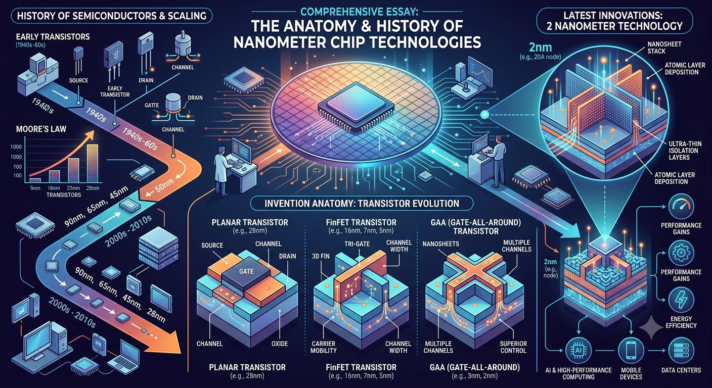
Nanometer (nm) semiconductor technology is one of humanity’s greatest engineering achievements. It combines physics, chemistry, materials science, electrical engineering, computer science, quantum mechanics, and artificial intelligence into one manufacturing ecosystem. Modern chips containing tens to hundreds of billions of transistors power smartphones, computers, vehicles, medical equipment, satellites, military systems, cloud computing, robotics, and AI.
The evolution from large micrometer-scale transistors in the 1960s to today’s 2 nm process technologies represents over sixty years of continuous innovation driven by Moore’s Law, Dennard scaling (historically), and relentless improvements in semiconductor fabrication.
Chapter 1: What Is a Nanometer?
A nanometer (nm) is:
1 nanometer = 0.000000001 meter (10⁻⁹ m)
Comparison:
- 1 meter = 1,000 millimeters
- 1 millimeter = 1,000 micrometers
- 1 micrometer = 1,000 nanometers
Therefore:
1 meter = 1,000,000,000 nanometers
For perspective:
- Human hair: 80,000–100,000 nm
- Red blood cell: ~7,000 nm
- DNA diameter: ~2.5 nm
- Silicon atom: ~0.2 nm
Modern chips are manufactured with structures only a few dozen silicon atoms wide.
Chapter 2: What Does “2 nm” Actually Mean?
Originally, process names closely matched transistor gate length.
Today, process names such as:
- 7 nm
- 5 nm
- 3 nm
- 2 nm
are technology-generation names rather than literal physical dimensions.
A “2 nm” process does not mean every transistor feature measures exactly 2 nanometers. Instead, it represents a generation offering:
- higher transistor density,
- lower power consumption,
- greater performance,
- improved manufacturing techniques.
Chapter 3: Before Nanometers
The first integrated circuits appeared in 1958–1959.
Early semiconductor manufacturing used dimensions measured in micrometers (µm):
- 50 µm
- 20 µm
- 10 µm
- 6 µm
These chips contained only dozens or hundreds of transistors.
Chapter 4: Birth of the Integrated Circuit
Two inventors independently created the integrated circuit:
- Jack Kilby (1958)
- Robert Noyce (1959)
Their invention eliminated the need for manually wiring thousands of discrete components together.
Chapter 5: Moore’s Law
In 1965, Gordon Moore observed that transistor counts on integrated circuits roughly doubled every two years.
This prediction guided the semiconductor industry for decades and motivated continual shrinking of transistor dimensions.
Chapter 6: The Evolution of Semiconductor Nodes
| Era | Process Node | Approximate Period | Major Innovation |
|---|---|---|---|
| 1970s | 10 µm | Early microprocessors | First commercial CPUs |
| 1980s | 3 µm | VLSI era | Increased integration |
| Late 1980s | 1 µm | CMOS maturity | Higher performance |
| 1990s | 800–350 nm | Personal computer boom | Faster CPUs |
| 2000 | 250–180 nm | Pentium era | Copper interconnects |
| 2002 | 130 nm | Larger caches | Improved lithography |
| 2004 | 90 nm | Lower voltages | Strained silicon |
| 2006 | 65 nm | Multi-core CPUs | Better efficiency |
| 2008 | 45 nm | High-k metal gate | Reduced leakage |
| 2010 | 32 nm | Smaller SRAM | Higher density |
| 2012 | 22 nm | FinFET transistors | 3D transistor structures |
| 2014 | 14/16 nm | Advanced FinFET | Mobile efficiency |
| 2016 | 10 nm | Denser layouts | Advanced patterning |
| 2018 | 7 nm | EUV introduction | AI acceleration |
| 2020 | 5 nm | High-density logic | Smartphones and AI |
| 2022 | 3 nm | Gate-all-around begins | Further efficiency gains |
| 2025–2026 | 2 nm | Nanosheet transistors | Next-generation computing |
Chapter 7: Anatomy of a Modern Semiconductor Chip
A modern chip contains multiple engineered layers:
- Silicon substrate
- Transistors
- Source and drain regions
- Gate dielectric
- Metal gate
- Contacts
- Local interconnects
- Copper wiring
- Low-k insulating materials
- Power delivery network
- Cache memory arrays
- Logic circuits
- Clock distribution
- Packaging
- Heat spreader
Each layer requires atomic-scale precision.
Chapter 8: Evolution of the Transistor
Planar MOSFET
Used from the 1960s until around 2011.
Advantages:
- Simple manufacturing
- Lower cost
Limitation:
- Increased leakage current at very small dimensions
FinFET (3D Transistor)
Introduced commercially at the 22 nm generation.
Advantages:
- Better electrostatic control
- Reduced leakage
- Higher speed
- Lower power
The gate wraps around a vertical silicon fin.
Gate-All-Around (GAA)
Commercialized beginning with 3 nm-class technologies and expanded at 2 nm.
Advantages:
- Gate surrounds the channel on all sides
- Better current control
- Lower leakage
- Higher transistor density
- Improved energy efficiency
Nanosheet Transistor
A form of GAA used in leading-edge 2 nm technologies.
Stacked horizontal silicon sheets carry current while the gate fully surrounds each sheet.
Chapter 9: How a Chip Is Manufactured
The manufacturing process includes:
- Growing ultra-pure silicon crystals
- Slicing wafers
- Polishing
- Oxidation
- Thin-film deposition
- Photoresist coating
- Photolithography
- Developing patterns
- Plasma etching
- Ion implantation
- Annealing
- Chemical-mechanical polishing
- Metallization
- Packaging
- Testing
A leading-edge chip may undergo hundreds to more than a thousand processing steps before shipment.
Chapter 10: Extreme Ultraviolet (EUV) Lithography
EUV uses light with a wavelength of approximately 13.5 nm.
It enables manufacturers to print much finer features than previous deep ultraviolet (DUV) systems, reducing the need for multiple patterning steps and improving manufacturing efficiency at advanced nodes.
Chapter 11: Why Smaller Nodes Matter
Benefits include:
- More transistors per chip
- Faster processing
- Lower energy consumption
- Larger on-chip memory
- Improved AI performance
- Longer battery life
- Higher computing density
Chapter 12: Challenges Below 5 nm
Engineers face:
- Quantum tunneling
- Heat removal
- Leakage current
- Atomic-scale manufacturing variability
- Extremely high fabrication costs
- Yield optimization
- Complex design verification
Chapter 13: The 2 nm Generation
Key characteristics include:
- Gate-all-around nanosheet transistors
- Higher transistor density than previous generations
- Improved performance at similar power, or lower power at similar performance (depending on design targets)
- Better support for AI, data centers, edge computing, and high-performance processors
Leading-edge 2 nm manufacturing also relies on advances in materials, packaging, design automation, and increasingly high numerical aperture (High-NA) EUV lithography for future scaling.
Chapter 14: Major Semiconductor Manufacturing Ecosystem
The semiconductor industry depends on a global ecosystem that includes:
- Chip designers
- Electronic design automation (EDA) software developers
- Silicon wafer suppliers
- Photolithography equipment manufacturers
- Materials and chemical suppliers
- Semiconductor foundries
- Packaging and testing companies
- Equipment manufacturers for deposition, etching, and metrology
This international supply chain spans North America, Europe, and Asia.
Chapter 15: Applications of Advanced Chips
Advanced semiconductor technologies power:
- Artificial intelligence
- Smartphones
- Personal computers
- Supercomputers
- Autonomous vehicles
- Medical imaging
- Robotics
- Financial systems
- Industrial automation
- Telecommunications
- Spacecraft
- Defense systems
- Scientific research
- Cloud computing
- Consumer electronics
Chapter 16: Future Beyond 2 nm
Researchers are exploring:
- High-NA EUV lithography
- Complementary FET (CFET) architectures
- Backside power delivery
- New channel materials such as 2D semiconductors
- Advanced 3D chip stacking
- Chiplet-based systems
- Silicon photonics
- Quantum computing hardware
- Neuromorphic computing
- Carbon-based and other post-silicon technologies
Future progress will likely depend as much on new transistor architectures, packaging, and system design as on simple dimensional scaling.
Conclusion
The history of nanometer chip technology is the story of continuous miniaturization, scientific innovation, and global collaboration. From the first integrated circuits containing only a handful of transistors to today’s 2 nm technologies with tens of billions of transistors, semiconductor engineering has transformed every aspect of modern society.
Although traditional transistor scaling has become increasingly difficult due to physical and economic limits, advances such as gate-all-around transistors, advanced lithography, heterogeneous integration, and new materials continue to push computing forward. The next era of semiconductor progress will be defined not only by smaller dimensions but also by smarter architectures, more efficient manufacturing, and tighter integration across hardware and software.





Be First to Comment