
Introduction
The race for AI dominance has spawned fundamentally different approaches to chip design. Google’s Tensor Processing Units (TPUs), NVIDIA’s GPUs, and AMD’s accelerators each reflect distinct philosophies about how to best handle the computational demands of modern machine learning and high-performance computing. Understanding these architectural differences reveals not just technical variations, but entirely different strategic visions for the future of computing.
Foundational Design Philosophy
NVIDIA: The Graphics Legacy
NVIDIA’s architecture stems from its graphics processing heritage. The company’s GPUs evolved from rendering pixels to performing parallel computations, and this DNA remains visible in their design. NVIDIA chips are built around the concept of thousands of relatively simple cores working simultaneously on different pieces of data—a paradigm known as Single Instruction, Multiple Data (SIMD).
The fundamental building block of modern NVIDIA architectures like Hopper and Blackwell is the Streaming Multiprocessor (SM). Each SM contains numerous CUDA cores, specialized tensor cores for matrix operations, and shared memory that allows cores within the SM to communicate efficiently. This hierarchical organization reflects NVIDIA’s need to balance generality with performance: the architecture must handle everything from video game rendering to scientific simulations to training neural networks.
AMD: The Challenger’s Efficiency
AMD’s approach with their Instinct line mirrors NVIDIA’s general philosophy but with crucial optimizations focused on memory efficiency and power consumption. AMD’s CDNA (Compute DNA) architecture represents a deliberate fork from their gaming-focused RDNA line, creating a design purely for data center computation.
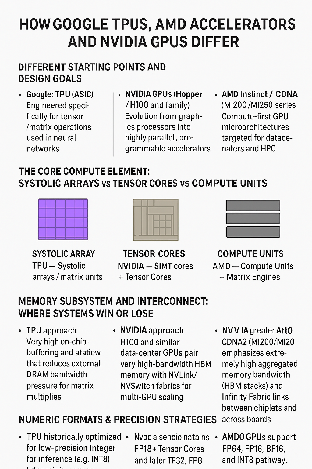
AMD organizes processing power into Compute Units (CUs), conceptually similar to NVIDIA’s SMs but with different internal configurations. The emphasis on memory bandwidth and the integration of high-bandwidth memory (HBM) directly into the chip package reflects AMD’s strategy of eliminating bottlenecks rather than simply adding more compute cores. Their Matrix Core units target the same tensor operations as NVIDIA’s Tensor Cores but often emphasize different precision formats and memory access patterns.
Google TPU: Purpose-Built for Neural Networks
Google took a radically different path. Rather than adapting existing architectures, they designed TPUs specifically for one purpose: neural network inference and training. This focus allowed them to strip away the flexibility that makes GPUs general-purpose and instead optimize relentlessly for matrix multiplication—the core operation in neural networks.
The TPU’s architecture centers around a massive systolic array, a grid of interconnected arithmetic logic units (ALUs) that data flows through in a wave-like pattern. Unlike GPUs where threads request data from memory, in a systolic array, data moves rhythmically through a fixed network of processors. This approach dramatically reduces the energy spent on memory access and instruction decoding, the two biggest power consumers in traditional processors.
Memory Architecture: The Critical Differentiator
NVIDIA’s Memory Hierarchy
NVIDIA GPUs employ a complex memory hierarchy designed for flexibility. At the top sits massive global memory (often 80GB or more of HBM in datacenter GPUs like the H100). Each SM has its own shared memory that threads within that SM can access quickly, plus registers for individual threads, and cache layers to speed up repeated memory accesses.
This hierarchy creates programming complexity but offers flexibility. Developers can explicitly control data placement in shared memory for maximum performance, or rely on caches for simpler programming models. The memory system must handle diverse access patterns: the strided accesses common in image processing, the random lookups in sparse computations, and the sequential streams typical of neural networks.
The bandwidth between compute and memory represents NVIDIA’s constant challenge. Even with HBM providing over 3TB/s of bandwidth in the H100, keeping thousands of cores fed with data requires sophisticated scheduling, compression, and caching strategies.
AMD’s Unified Memory Approach
AMD has made memory architecture a competitive differentiator. Their Infinity Fabric interconnect technology creates unified memory spaces across multiple dies and even multiple chips. This allows AMD to scale memory capacity and bandwidth more flexibly than competitors.
The MI300 series demonstrates this philosophy, combining CPU and GPU dies with shared HBM pools. This unified memory approach reduces data copying between different types of processors and simplifies programming models for heterogeneous computing. Where NVIDIA requires explicit data transfers between CPU and GPU memory spaces, AMD’s architecture can allow both to access the same physical memory.
AMD’s memory controllers also implement sophisticated compression algorithms and prefetching mechanisms, attempting to predict what data will be needed and staging it efficiently. Their emphasis on memory subsystem efficiency over raw core count reflects a bet that memory bandwidth, not compute throughput, will be the primary bottleneck for AI workloads.
TPU’s Memory-Centric Design
Google’s TPU takes the most radical approach to memory. The systolic array architecture minimizes memory accesses by maximizing data reuse. Once a weight matrix is loaded into the array, it can be multiplied against thousands of activation vectors with minimal additional memory traffic.
TPUs also feature a unique memory called High Bandwidth Memory (HBM) positioned extremely close to the compute elements. Unlike GPUs where memory sits across a relatively long bus, TPU memory is directly adjacent to processing elements, reducing both latency and power consumption.
The unified buffer in TPU architecture acts as both cache and scratchpad, carefully orchestrated by specialized compilers. Rather than relying on general-purpose cache replacement policies, the TPU compiler analyzes the entire neural network graph and schedules memory movements to minimize traffic and maximize data locality.
Compute Precision and Data Types
The Precision Revolution
One of the most significant architectural differences lies in how these chips handle numerical precision. Traditional computing used 32-bit or 64-bit floating-point numbers, but AI training and inference often work effectively with much lower precision.
NVIDIA has progressively added support for multiple data types. Their Tensor Cores can compute in FP64, FP32, TF32 (a custom 19-bit format), FP16, BF16 (bfloat16), INT8, INT4, and even FP8 formats. This flexibility allows developers to choose precision based on their specific accuracy requirements, with lower precision enabling dramatically higher throughput.
AMD’s approach is similar, with Matrix Cores supporting various precision levels, though the specific formats and relative performance characteristics differ. AMD has particularly emphasized BF16 and INT8 performance, targeting popular training and inference scenarios.
Google’s TPUs were pioneers in mixed-precision computing. Early versions supported only INT8 for inference, deliberately sacrificing flexibility for efficiency. Later versions added BF16 for training, but the choices remain more constrained than GPUs. This reflects Google’s philosophy: by limiting precision options to those that actually matter for neural networks, the hardware can be simpler, faster, and more power-efficient.
Interconnect and Scaling Architecture
NVIDIA’s NVLink and NVSwitch
NVIDIA recognized early that single-chip performance wouldn’t suffice for the largest AI models. Their NVLink technology creates high-bandwidth connections between GPUs, allowing them to share memory and coordinate computation. The latest generation provides bidirectional bandwidth of 900GB/s between GPU pairs.
For larger deployments, NVIDIA developed NVSwitch, essentially a specialized router that allows any GPU to communicate with any other at full NVLink speed. This enables configurations like the DGX SuperPOD where hundreds of GPUs work together as a unified system.
This interconnect architecture reflects NVIDIA’s vision of distributed AI training where models are partitioned across many chips. The architecture must handle both data parallelism (different chips processing different training examples) and model parallelism (different chips processing different parts of the model).
AMD’s Infinity Fabric
AMD’s Infinity Fabric serves a similar purpose but with a different philosophy. Rather than being GPU-specific, Infinity Fabric connects CPUs, GPUs, and other accelerators in a heterogeneous mesh. This reflects AMD’s strategy of offering complete system solutions rather than just GPUs.
The Infinity Fabric topology tends toward mesh networks rather than NVIDIA’s switch-based approach, which can provide more predictable latency characteristics but potentially less bisection bandwidth. AMD’s recent MI300 systems feature extremely tight integration between different compute elements, effectively creating superchips with thousands of compute cores of different types.
TPU’s Custom Interconnect
Google’s approach to interconnect is the most specialized. TPU pods connect individual TPU chips through a custom 3D mesh topology where each chip connects directly to six neighbors. This topology is specifically optimized for neural network operations, where certain communication patterns (like all-reduce operations in distributed training) are extremely common.
The interconnect is tightly integrated with the compiler toolchain. Google’s XLA compiler can analyze a neural network, determine optimal sharding strategies, and generate code that efficiently uses the interconnect to minimize communication overhead. This compiler-hardware co-design achieves efficiency that would be difficult with more general-purpose interconnects.
Importantly, TPU interconnect bandwidth is sufficient to make distributed training efficient at scales that would be impractical for other architectures. Google routinely trains models across thousands of TPU cores, with the interconnect and compilation strategy ensuring that communication doesn’t become a bottleneck.
Programming Models and Software Ecosystems
NVIDIA CUDA: The Ecosystem Advantage
NVIDIA’s greatest advantage may not be hardware at all—it’s CUDA. Introduced in 2006, CUDA provides a relatively accessible programming model for GPU computing. Developers write C++ code with special extensions, and the CUDA compiler generates efficient GPU code.
The CUDA ecosystem extends far beyond the language itself. Libraries like cuDNN for deep learning, cuBLAS for linear algebra, and cuFFT for signal processing provide optimized implementations of common operations. Frameworks like PyTorch and TensorFlow have deep CUDA integration, making NVIDIA GPUs the default choice for many AI researchers.
This software moat is difficult to overcome. Even when competitors offer superior hardware, the effort required to port and optimize software for a new platform represents a significant barrier.
AMD ROCm: The Open Alternative
AMD’s ROCm (Radeon Open Compute) platform takes an open-source approach to GPU computing. ROCm includes HIP, a programming language designed to be source-compatible with CUDA, allowing relatively straightforward porting of CUDA applications.
The open-source nature of ROCm appeals to institutions concerned about vendor lock-in and aligns with AMD’s strategy of positioning itself as the more open alternative to NVIDIA. However, ROCm’s ecosystem remains less mature, with fewer optimized libraries and less comprehensive framework support.
AMD has invested heavily in improving ROCm compatibility with popular AI frameworks, but the gap in software maturity represents a significant challenge. Many cutting-edge models and techniques appear first on NVIDIA hardware simply because that’s where the researchers and developers are.
TPU: Compiler-First Philosophy
Google’s approach to TPU programming is fundamentally different. Rather than exposing the hardware directly to developers, Google provides high-level frameworks (like TensorFlow and JAX) that compile to TPU instructions.
The XLA (Accelerated Linear Algebra) compiler is the heart of this approach. XLA takes high-level descriptions of computations, performs aggressive optimizations, and generates efficient TPU code. This compiler-first philosophy allows Google to change hardware details between TPU generations without breaking user code.
The trade-off is that TPUs are essentially accessible only through Google’s frameworks and cloud services. There’s no equivalent of CUDA where developers can write low-level code targeting the hardware directly. This limits flexibility but ensures that code running on TPUs has been heavily optimized by Google’s expert compiler engineers.
Power Efficiency and Performance per Watt
The Energy Equation
As AI models grow, power consumption has become a critical constraint. Data center power budgets limit how many chips can be deployed, and power delivery and cooling represent major infrastructure investments.
NVIDIA’s latest GPUs like the H100 consume up to 700W per chip under full load. This massive power draw reflects the architectural choice to maximize performance, accepting high power consumption as a necessary cost. NVIDIA argues that higher absolute performance justifies the power consumption because workloads complete faster.
AMD has traditionally emphasized performance per watt as a competitive advantage, with chips like the MI300 designed to deliver similar performance to NVIDIA counterparts while consuming less power. This efficiency comes from various architectural choices: better memory compression, more efficient interconnects, and silicon process optimizations.
Google’s TPUs represent the extreme of efficiency-focused design. By optimizing specifically for neural networks and using systolic arrays that minimize memory movement, TPUs achieve dramatically higher performance per watt for their target workloads. A TPU v4 pod delivers multiple exaflops of compute with power consumption that would only support a fraction of equivalent GPU capacity.
Specialized Units for Efficiency
All three vendors have added specialized units for specific operations, recognizing that general-purpose processing is inherently inefficient.
NVIDIA’s Tensor Cores are dedicated matrix multiplication engines that operate at much higher throughput than general CUDA cores for these operations. The Hopper generation added a Transformer Engine specifically optimized for attention mechanisms, the core operation in modern language models.
AMD’s Matrix Cores serve a similar purpose, with specific optimizations for the sparse matrix operations that appear in certain neural network types.
Google’s entire TPU design is essentially a specialized unit, with every transistor dedicated to neural network operations. This extreme specialization enables industry-leading efficiency but only for the target workload.
Real-World Performance Characteristics
Training Large Language Models
For training massive language models like GPT or Gemini, different architectures show distinct characteristics. NVIDIA’s GPUs excel at the exploratory phase where researchers experiment with different architectures and hyperparameters, thanks to the flexibility of CUDA and the mature software ecosystem.
AMD systems can offer competitive performance once code is optimized, potentially with better power efficiency. However, the software maturity gap means getting optimal performance requires more engineering effort.
Google’s TPU pods arguably achieve the best performance-per-dollar and performance-per-watt for training at scale, but only when using Google’s frameworks and cloud infrastructure. The compiler-first approach means less time spent on low-level optimization, but the lack of flexibility can be limiting for novel architectures.
Inference at Scale
For serving trained models—inference—the architectural differences become even more pronounced. Inference often prioritizes latency (response time) over throughput, and power efficiency matters enormously when serving billions of requests.
NVIDIA’s GPUs handle inference well, with features like dynamic batching that group multiple requests together for efficiency. Their broad software support means virtually any model can be deployed.
AMD offers competitive inference performance with potentially better efficiency, though software limitations can be challenging.
TPUs shine particularly bright in inference scenarios. The systolic array architecture that seemed specialized for training proves even more beneficial for inference, where the same model parameters are reused across countless inputs. Google’s services handling web search, ads, and other massive-scale inference tasks run primarily on TPUs, demonstrating their effectiveness at this task.
Scientific Computing and HPC
Beyond AI, many scientific workloads need massive computational power. Here the general-purpose nature of GPUs provides advantages.
NVIDIA GPUs dominate scientific computing, with their CUDA ecosystem offering libraries for everything from molecular dynamics to climate simulation. The flexibility to handle arbitrary computational patterns and well-optimized math libraries makes them the default choice.
AMD has made inroads in HPC with competitive performance and open-source software appealing to academic and government institutions. Their unified memory architecture can simplify certain types of simulations.
TPUs are essentially irrelevant for traditional HPC. Their specialization for neural networks means they cannot efficiently handle the diverse computational patterns in scientific codes. This represents the fundamental trade-off: extreme efficiency for one workload type means inefficiency for others.
Manufacturing and Process Technology
Silicon Process Nodes
All three vendors depend on cutting-edge semiconductor manufacturing, primarily from TSMC. NVIDIA’s H100 uses TSMC’s 4nm process, AMD’s MI300 uses 5nm and 6nm chiplets, and Google’s TPU v4 uses 7nm.
The specific process node doesn’t tell the whole story—architectural efficiency matters as much as transistor density. Google achieves competitive or superior efficiency despite using a slightly older process because the TPU architecture inherently requires fewer transistors for the same computational task.
Chiplet Strategies
Both AMD and NVIDIA have embraced chiplet architectures where multiple silicon dies are combined into a single package. This allows them to work around the physical limitations of monolithic chips and achieve better manufacturing yields.
AMD’s MI300 represents an aggressive chiplet strategy, combining CPU and GPU dies with HBM memory stacks all in one package. This integration reduces communication latency and power consumption while allowing independent optimization of different components.
NVIDIA’s approach has been more conservative, but the coming Blackwell architecture features dual GPU dies connected by an extremely high-bandwidth link, effectively creating a single logical GPU from two physical chips.
Google’s approach to TPUs has varied. Some generations use monolithic designs for simplicity and efficiency, while others employ chiplet strategies when the benefits justify the additional complexity.
The Ecosystem Beyond the Chip
Cloud Integration
The business model around these chips significantly affects their design. NVIDIA sells to everyone—cloud providers, enterprises, researchers—so their chips must work in diverse environments.
AMD follows a similar model, positioning their chips as drop-in alternatives to NVIDIA with the appeal of lower cost or higher efficiency.
Google’s TPUs exist primarily as a cloud service. This changes the design calculus entirely. Google doesn’t need to worry about third-party software compatibility or diverse deployment scenarios. They optimize for their own workloads and infrastructure, achieving efficiency that would be impossible with a more general-purpose product.
The Software Development Kit Battle
Beyond the core programming models, each vendor provides extensive SDKs, profiling tools, debugging utilities, and optimization guides. NVIDIA’s ecosystem is the most mature, with tools like Nsight for profiling and NGC (NVIDIA GPU Cloud) providing optimized container images.
AMD’s tools are catching up but remain less comprehensive. The open-source nature appeals to some developers but can mean slower support for cutting-edge features.
Google’s TPU tools integrate tightly with their cloud platform and frameworks. The profiler can show exactly which operations are memory-bound versus compute-bound and suggest specific optimizations, but only within Google’s ecosystem.
Future Trajectories
NVIDIA’s AI Dominance
NVIDIA’s strategy centers on maintaining their CUDA software moat while pushing hardware performance boundaries. Each generation adds new specialized units (like the Transformer Engine) targeting emerging AI techniques. Their DGX systems and cloud partnerships aim to make NVIDIA the default choice for AI at any scale.
The risk for NVIDIA is that their general-purpose architecture may lose efficiency advantages as competitors specialize further. The enormous power consumption of their latest chips also creates challenges as data centers hit power limits.
AMD’s Efficiency Play
AMD positions itself as the efficient, open alternative. Their unified CPU-GPU architecture and emphasis on memory bandwidth target workloads where data movement dominates compute. Success depends on maturing their software ecosystem enough to overcome NVIDIA’s developer advantage.
AMD’s strategy of tighter integration between different compute elements may prove prescient as AI models grow. The ability to efficiently share memory between CPUs and GPUs could enable new architectural patterns.
Google’s Vertical Integration
Google continues pushing TPU specialization, with each generation adding optimizations for their specific workloads. Their vertical integration—controlling the chip, compiler, frameworks, and cloud infrastructure—allows optimizations impossible for competitors.
The limitation is that TPUs serve only Google’s ecosystem. They’ve opened TPUs to cloud customers, but the lack of CUDA-style flexibility means TPUs will remain a specialized solution rather than a general-purpose platform.
Conclusion
The architectural differences between Google TPUs, AMD GPUs, and NVIDIA GPUs reflect fundamentally different philosophies about computing’s future. NVIDIA bets on flexible, general-purpose accelerators with a rich software ecosystem. AMD offers an alternative emphasizing efficiency and openness while maintaining broad compatibility. Google pursues extreme specialization for neural networks, sacrificing flexibility for unmatched efficiency in their target domain.
None of these approaches is universally superior. NVIDIA’s flexibility and ecosystem make them the default choice for most AI workloads. AMD provides competitive alternatives with potential cost and efficiency advantages. Google’s TPUs deliver unbeatable efficiency for neural networks at scale but only within their ecosystem.
As AI continues evolving, we may see convergence as successful ideas propagate across architectures, or further divergence as vendors double down on their distinct advantages. The enormous investments all three companies are making suggest that specialized AI accelerators will remain central to computing infrastructure for years to come, with architectural diversity reflecting the diverse needs of different users and workloads.


Be First to Comment