
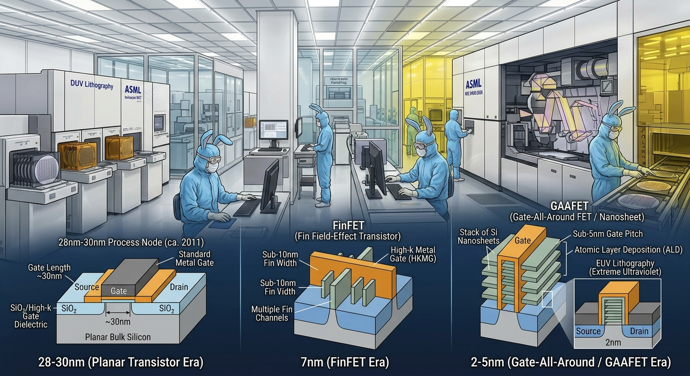
The progression from 30/28 nm to 7 nm, 5 nm and 2 nm represents one of the most important technological transformations in modern computing. It is not simply a story of making a transistor physically smaller. Each generation requires changes to transistor architecture, materials, lithography, electrical design, interconnects, power delivery, manufacturing, electronic-design automation (EDA), packaging, and thermal engineering.
A crucial point is that the names 28 nm, 7 nm, 5 nm and 2 nm are process-node names, not literal measurements of every feature on a modern chip. Modern node names are better understood as identifiers for generations of semiconductor manufacturing technology.
1. Introduction: What Is a Semiconductor Chip?
A semiconductor chip, or integrated circuit (IC), is a microscopic system containing potentially billions of electronic devices interconnected to perform computation, memory, communication, sensing or control.
At its most fundamental level, a digital processor consists of:
Transistors → logic gates → circuits → functional blocks → cores/accelerators → system-on-chip (SoC).
A simplified hierarchy is:
Electronic system
       ↓
Package
       ↓
Chip / SoC
       ↓
Functional blocks
       ↓
Logic gates
       ↓
Transistors
       ↓
Semiconductor devices
       ↓
Silicon wafer
The extraordinary achievement of semiconductor engineering is that these structures can be manufactured repeatedly and precisely across an entire wafer.
2. From 28 nm to 2 nm: The Evolution at a Glance
| Approximate generation | Typical transistor architecture | Major technological direction |
|---|---|---|
| 28/30 nm | Planar MOSFET | Mature planar CMOS |
| 16/14/10 nm | FinFET | 3D transistor architecture |
| 7 nm | Advanced FinFET | Heavy scaling + EUV transition |
| 5 nm | Advanced FinFET | Extensive EUV + greater density |
| 3 nm | FinFET and/or GAA depending on manufacturer | GAA transition |
| 2 nm class | Gate-All-Around nanosheet/ribbon transistor | GAA + advanced interconnect/power |
This evolution is important because the transistor itself eventually becomes unable to scale efficiently using its previous architecture.
3. The 28/30 nm Era: The Final Great Planar Generation
At approximately the 28 nm generation, traditional planar CMOS technology was still an important manufacturing architecture.
A simplified planar transistor looks conceptually like:
             Gate
          ┌─────────┐
          │         │
          └─────────┘
              │
Source ───── Channel ───── Drain
              │
        Silicon substrate
The gate controls the electrical conductivity of the channel between source and drain.
Why planar scaling eventually became difficult
As dimensions became smaller:
- leakage increased;
- short-channel effects became more severe;
- controlling the transistor became harder;
- voltage could not simply continue decreasing indefinitely;
- transistor-to-transistor variation became increasingly important;
- power density became a major problem.
Consequently, the industry moved toward a three-dimensional transistor structure.
4. The FinFET Revolution
The answer was the FinFET, in which the conducting channel rises vertically from the silicon surface.
Conceptually:
             Gate
        ┌─────────────┐
        │             │
        │    FIN      │
        │    ││       │
────────┴────││───────┴──────
             ││
          Silicon
         substrate
Instead of controlling a flat channel primarily from above, the gate surrounds multiple sides of the fin.
This provides substantially better electrostatic control.
FinFET became fundamental to generations including advanced 14/16 nm, 10 nm, 7 nm and 5 nm technologies.
5. 7 nm: A Major Manufacturing Transition
The 7 nm generation represents a major stage in semiconductor scaling.
The transistor itself remained fundamentally based on FinFET technology for major foundry implementations, but the manufacturing ecosystem became dramatically more sophisticated.
The chip designer now had to simultaneously optimize:
- transistor dimensions;
- standard-cell architecture;
- metal layers;
- contact structures;
- routing;
- power distribution;
- clock networks;
- SRAM;
- cache;
- libraries;
- lithography;
- yield;
- thermal characteristics.
EUV becomes increasingly important
Extreme ultraviolet lithography uses approximately 13.5 nm wavelength light to print extremely small patterns.
The transition to EUV reduced the dependence on some extremely complex multiple-patterning techniques for selected layers.
6. 5 nm: Increasing Density and EUV Integration
TSMC states that its N5 technology entered volume production in 2020 and was its second generation using EUV lithography. (TSMC)
At 5 nm, the architecture becomes substantially more sophisticated.
A modern chip is not simply:
transistor + transistor + transistor.
It is a multilayer three-dimensional manufacturing structure containing:
- transistor regions;
- contacts;
- local interconnect;
- multiple metal layers;
- dielectric materials;
- vias;
- power networks;
- clock networks;
- signal networks.
Conceptually:
        TOP OF CHIP
────────────────────────
     Upper metal layers
────────────────────────
       Metal routing
────────────────────────
        Vias
────────────────────────
   Local interconnect
────────────────────────
      Transistors
────────────────────────
    Silicon substrate
        BOTTOM
The chip therefore becomes a three-dimensional electrical infrastructure.
7. The Difference Between “5 nm” and Physical Reality
One of the most important misconceptions is:
“A 5 nm chip has everything measuring 5 nm.”
That is not correct.
A process-node number is a technology-generation designation. Different physical dimensions—such as gate length, contacted pitch, metal pitch and SRAM dimensions—have different values.
Therefore:
5 nm ≠ every transistor feature is 5 nm.
The same principle applies even more strongly to 3 nm and 2 nm-class technologies.
8. 3 nm: The Beginning of a New Transistor Era
At the 3 nm generation, the industry reaches another important architectural boundary.
Some manufacturers continued refining FinFET technology, while others began moving to Gate-All-Around (GAA) architectures.
TSMC reports that its N3 technology entered high-volume production in 2022 and is based on FinFET technology. (TSMC)
This illustrates an important point:
A node name does not uniquely determine transistor architecture.
Two companies can call their technologies “3 nm” while using different transistor structures.
9. Gate-All-Around Transistors
The GAA transistor represents the next major architectural evolution after FinFET.
Instead of the gate controlling the channel from three principal sides, the gate surrounds the channel.
Conceptually:
             GATE
       ┌───────────────┐
       │ ┌───────────┐ │
       │ │ CHANNEL   │ │
       │ └───────────┘ │
       └───────────────┘
             GATE
This gives the gate much stronger electrostatic control over the channel.
The result can include:
- reduced leakage;
- improved control of short-channel effects;
- better low-voltage operation;
- greater transistor scaling flexibility;
- improved performance-per-watt.
10. Nanosheet Transistors
One important implementation of GAA is the nanosheet transistor.
Instead of one vertical fin, multiple horizontal semiconductor sheets can be stacked.
Conceptually:
          Gate surrounds sheets

        ┌───────────────────┐
        │   ─────────────    │
        │   ─────────────    │
        │   ─────────────    │
        │   ─────────────    │
        └───────────────────┘
              Gate
The channel width can be adjusted by changing the dimensions and number of nanosheets.
This provides designers with greater flexibility in balancing:
performance ↔ power ↔ area.
11. The 2 nm Generation
The move toward 2 nm-class technology represents another major architectural transition.
For example, TSMC’s N2 technology uses a first-generation nanosheet transistor architecture. TSMC reports that N2 is designed for a 15% speed increase at the same power or a 30% power reduction at the same speed versus its previous-generation 3 nm technology, along with more than 1.15× chip-density improvement. (TSMC Research)
The fundamental change can therefore be summarized:
28 nm
   ↓
Planar transistor

7 nm
   ↓
FinFET

5 nm
   ↓
Advanced FinFET

3 nm
   ↓
Advanced FinFET / GAA transition

2 nm
   ↓
GAA nanosheet / ribbon transistor
12. How a 2 nm-Class Transistor Is Architected
A simplified nanosheet transistor can be visualized as:
                 GATE
        ┌───────────────────┐
        │ ┌───────────────┐ │
Source ─┤ │  Nanosheet 1  │ ├─ Drain
        │ ├───────────────┤ │
        │ │  Nanosheet 2  │ │
        │ ├───────────────┤ │
        │ │  Nanosheet 3  │ │
        │ └───────────────┘ │
        └───────────────────┘
                 GATE
The gate surrounds the channels.
This is fundamentally different from the earlier planar architecture.
13. The Chip Is More Than the Transistor
A processor contains several interconnected architectural layers.
Layer 1 — Device
The transistor.
Layer 2 — Logic
Examples:
- AND;
- OR;
- NOT;
- NAND;
- NOR;
- XOR.
Layer 3 — Sequential logic
Examples:
- flip-flops;
- registers;
- counters;
- state machines.
Layer 4 — Functional units
Examples:
- ALUs;
- floating-point units;
- vector engines;
- AI accelerators;
- memory controllers.
Layer 5 — Processor architecture
Examples:
- CPU cores;
- GPU cores;
- NPU engines;
- cache hierarchy.
Layer 6 — SoC
The complete system may contain:
- CPU;
- GPU;
- NPU;
- memory controllers;
- security engines;
- I/O;
- communication interfaces.
14. Designing the Chip Before Manufacturing
The physical chip begins as an electronic design.
A simplified process is:
Product requirements
       ↓
Computer architecture
       ↓
Microarchitecture
       ↓
RTL design
       ↓
Functional verification
       ↓
Logic synthesis
       ↓
Physical design
       ↓
Place & route
       ↓
Timing/power analysis
       ↓
Tape-out
       ↓
Mask generation
       ↓
Wafer manufacturing
       ↓
Packaging
       ↓
Testing
This means a semiconductor company can spend years designing a chip before the first production wafer is manufactured.
15. EDA: The Invisible Architecture Behind the Chip
Modern chips cannot realistically be designed manually transistor-by-transistor.
Electronic Design Automation (EDA) software is essential.
EDA tools help with:
- RTL development;
- synthesis;
- simulation;
- timing analysis;
- floorplanning;
- placement;
- routing;
- physical verification;
- power analysis;
- design-rule checking;
- mask preparation.
The designer therefore creates an enormous digital description that is progressively transformed into a physical layout.
16. Floorplanning
Before placing billions of transistors, designers decide where major blocks should go.
A simplified processor floorplan might look like:
┌──────────────────────────────────────┐
│ CPU │ CPU │ CPU │      GPU          │
│     │     │     │                   │
├─────┼─────┼─────┼───────────────────┤
│ Cache            │   AI / NPU       │
│                  │                  │
├──────────────────┼──────────────────┤
│ Memory Controller│ I/O / Security   │
└──────────────────────────────────────┘
The physical layout affects:
- speed;
- power;
- heat;
- manufacturing yield;
- package design.
17. Standard Cells
Digital chips are constructed using libraries of standard cells.
Examples include:
- NAND;
- NOR;
- inverter;
- flip-flop;
- multiplexer.
The chip designer combines these cells into increasingly complex systems.
At advanced nodes, standard-cell architecture itself becomes a major engineering discipline because transistor density, routing resources and power distribution are tightly coupled.
18. Interconnect Becomes a Major Problem
As transistors become faster and smaller, the wires connecting them become increasingly important.
A simplified hierarchy is:
Transistor
   ↓
Contact
   ↓
Local interconnect
   ↓
Lower metal layers
   ↓
Intermediate metal layers
   ↓
Upper metal layers
   ↓
Package
Electrical delay is not determined solely by the transistor.
It also depends heavily on:
resistance + capacitance + interconnect length.
This is called RC delay.
Consequently, advanced semiconductor engineering increasingly becomes an interconnect problem as well as a transistor problem.
19. Power Delivery
Every transistor needs electrical power.
Traditionally, power and signal routing share much of the front-side interconnect infrastructure.
As chips become denser, this creates congestion.
A major modern solution is backside power delivery.
Intel’s 18A technology combines RibbonFET GAA transistors with PowerVia backside power delivery. Intel explains that PowerVia relocates significant power-delivery structures to the backside of the die, freeing front-side routing resources for signals. (Intel)
Conceptually:
        FRONT SIDE
 ┌───────────────────────────┐
 │ Signal interconnects      │
 │ Logic                     │
 │ Transistors               │
 └───────────────────────────┘
              │
       Silicon / vias
              │
 ┌───────────────────────────┐
 │ BACKSIDE POWER NETWORK    │
 └───────────────────────────┘
This is an important example of how advanced-node scaling increasingly requires system-level architectural changes, not merely smaller transistors.
20. Lithography: Printing the Chip
Lithography transfers patterns onto semiconductor wafers.
A simplified process is:
Design data
     ↓
Mask
     ↓
Light
     ↓
Optical system
     ↓
Photoresist
     ↓
Silicon wafer
EUV lithography uses approximately 13.5 nm wavelength radiation.
The lithography machine must position and expose structures with extraordinary precision.
21. High-NA EUV
The next stage is High Numerical Aperture EUV, commonly called High-NA EUV.
Increasing numerical aperture improves imaging resolution.
This is part of the industry’s effort to continue scaling advanced semiconductor manufacturing.
The transition is not simply:
“use a smaller laser.”
It involves changes throughout:
- optics;
- masks;
- photoresists;
- metrology;
- process control;
- computational lithography;
- design rules.
22. Building the Chip Layer by Layer
A chip is effectively constructed through repeated cycles of:
- depositing material;
- coating;
- exposing;
- developing;
- etching;
- cleaning;
- implanting/doping;
- planarizing;
- inspecting;
- repeating.
Conceptually:
Material deposition
        ↓
Photoresist
        ↓
Lithography
        ↓
Development
        ↓
Etching
        ↓
Cleaning
        ↓
Inspection
        ↓
Next layer
These operations are repeated many times.
23. Chemical Mechanical Planarization
One important process is chemical mechanical planarization (CMP).
It creates a sufficiently flat surface so that subsequent layers can be manufactured accurately.
Without precise planarization, microscopic variations accumulate through the stack.
At advanced nodes, controlling these variations becomes increasingly difficult.
24. Transistor Formation
The transistor requires carefully controlled semiconductor regions.
The manufacturing process involves:
- semiconductor deposition;
- selective etching;
- doping or other electrical-property engineering;
- dielectric formation;
- gate formation;
- contacts;
- source/drain structures.
The objective is to create a device that switches predictably billions of times.
25. From FinFET to GAA: Why the Architecture Changes
The progression can be understood through electrostatic control.
Planar
       Gate
       ↓↓↓
──────────────
   Channel
──────────────
FinFET
      Gate
    ↙ ↓ ↓ ↘
      FIN
      ││
      ││
GAA
   ┌───────────┐
   │  CHANNEL  │
   └───────────┘
      ↑ GATE
   surrounding
The goal is increasingly precise control of the channel.
26. Materials Engineering
Advanced semiconductor manufacturing involves many materials, including:
- silicon;
- silicon-germanium;
- silicon dioxide;
- high-k dielectrics;
- metals;
- low-k dielectrics;
- barrier materials;
- advanced photoresists.
At extremely small dimensions, material properties become critical.
A tiny defect that might have been insignificant at an older node can potentially affect an advanced device.
27. SRAM and Memory Become Critical
A processor is not composed entirely of logic.
It also requires enormous quantities of memory structures.
Examples include:
- registers;
- L1 cache;
- L2 cache;
- L3 cache;
- SRAM arrays.
SRAM scaling is one of the major challenges in advanced-node technology.
The logic transistor may improve significantly while memory scaling follows a different trajectory.
28. Thermal Architecture
Smaller transistors do not automatically mean cooler processors.
Modern high-performance chips can contain enormous numbers of transistors switching at high frequency.
Therefore:
Transistor density
       ↓
Computational density
       ↓
Power density
       ↓
Heat generation
       ↓
Thermal engineering
Thermal design includes:
- die-level heat spreading;
- package materials;
- heat spreaders;
- cooling systems;
- workload management;
- voltage/frequency control.
29. Packaging Becomes Part of the Architecture
The chip itself is only one part of the system.
Modern advanced computing increasingly uses:
- chiplets;
- 2.5D integration;
- 3D stacking;
- high-bandwidth memory;
- advanced substrates;
- hybrid bonding;
- through-silicon vias.
Therefore the future of semiconductor scaling is moving from:
“How small can one transistor become?”
toward:
“How efficiently can an entire computing system be integrated?”
Intel, for example, describes advanced packaging and 3D integration alongside its 18A process technology. (Intel)
30. Chiplets
Instead of manufacturing one enormous monolithic die, designers can divide the system into multiple dies.
┌─────────────┐ ┌─────────────┐
│ CPU Chiplet │ │ CPU Chiplet │
└─────────────┘ └─────────────┘
       │               │
       └──────┬────────┘
              ↓
      ┌──────────────┐
      │ I/O Chiplet  │
      └──────────────┘
              │
      ┌──────────────┐
      │ Memory/HBM   │
      └──────────────┘
Advantages can include:
- manufacturing flexibility;
- improved yield economics;
- reusable IP;
- heterogeneous process technologies;
- larger overall systems.
This is especially important for AI and high-performance computing.
31. Why 2 nm Is Not the End
The semiconductor industry does not stop at 2 nm.
Scaling increasingly depends on combining:
new transistor architectures + new materials + new lithography + backside power + advanced interconnect + 3D integration + chiplets + packaging.
Intel’s current roadmap already extends beyond 18A toward 14A, with RibbonFET 2 and PowerDirect technologies. (Intel)
This illustrates the broader direction: future scaling is becoming a system architecture problem.
32. Comparing the Generations
| Feature | 28 nm | 7 nm | 5 nm | 2 nm class |
|---|---|---|---|---|
| Basic transistor family | Planar | FinFET | FinFET | GAA |
| Channel control | Moderate | Strong | Stronger | Very strong |
| EUV importance | Low/limited | Increasing | Major | Major/next-generation |
| Density | High for its era | Much higher | Higher | Extremely high |
| Interconnect challenge | Significant | Severe | Very severe | Critical |
| Power delivery | Front-side | Front-side | Front-side | Increasing backside integration |
| Packaging importance | Moderate | High | Very high | Critical |
| Design complexity | High | Very high | Extreme | Extreme |
33. The Complete Architecture of an Advanced Chip
The modern semiconductor can therefore be understood as a stack:
                 SOFTWARE
                    ↓
             System architecture
                    ↓
             CPU/GPU/NPU design
                    ↓
              RTL / logic
                    ↓
              Standard cells
                    ↓
             Physical layout
                    ↓
          Transistor architecture
                    ↓
       Interconnect + power network
                    ↓
          Semiconductor layers
                    ↓
              Silicon wafer
                    ↓
                Packaging
                    ↓
             Cooling system
                    ↓
             COMPLETE SYSTEM
This is why a 2 nm processor is not simply a “smaller 28 nm processor.”
It represents an entirely different level of device, manufacturing and system co-optimization.
34. Design-Technology Co-Optimization
Modern semiconductor development increasingly relies on DTCO — Design-Technology Co-Optimization.
The fundamental principle is:
The transistor process and the chip architecture must be designed together.
For example, changing transistor architecture can affect:
- standard cells;
- routing;
- power distribution;
- SRAM;
- clocking;
- performance;
- thermal characteristics.
Therefore the foundry and chip designer cannot treat manufacturing technology as completely independent from chip design.
35. System-Technology Co-Optimization
The next step is broader:
STCO — System-Technology Co-Optimization.
Instead of optimizing only:
transistor → chip
engineers optimize:
transistor → die → chiplet → package → memory → system.
This is particularly important for AI accelerators and high-performance computing.
36. Why Scaling Has Become More Difficult
The historical semiconductor scaling model was approximately:
Smaller transistor
       ↓
More transistors
       ↓
Higher performance
       ↓
Lower cost per function
Today the relationship is more complicated.
Engineers must simultaneously solve:
Density
   +
Performance
   +
Power
   +
Heat
   +
Interconnect
   +
Yield
   +
Manufacturing cost
   +
Packaging
Improving one dimension can make another more difficult.
37. The Economics of 2 nm
Advanced-node manufacturing requires enormous capital investment.
A leading-edge semiconductor ecosystem requires:
- fabrication plants;
- lithography systems;
- deposition equipment;
- etch equipment;
- metrology;
- inspection;
- chemical supply chains;
- silicon wafers;
- mask technology;
- EDA software;
- intellectual property;
- packaging facilities;
- highly trained engineers.
Consequently, only a small number of organizations can manufacture the most advanced logic technologies at enormous scale.
38. The Global Semiconductor Ecosystem
The advanced-chip industry is not controlled by one company.
It is an ecosystem involving:
Chip designers
Companies designing CPUs, GPUs, AI accelerators and SoCs.
Foundries
Companies manufacturing chips for themselves or customers.
EDA companies
Companies providing design software.
Lithography companies
Companies producing critical lithography systems.
Equipment manufacturers
Providing:
- deposition;
- etching;
- inspection;
- metrology;
- cleaning;
- packaging equipment.
Materials companies
Producing:
- photoresists;
- gases;
- chemicals;
- wafers;
- specialty materials.
39. Why the Journey From 28 nm to 2 nm Matters
The technological progression can be represented as:
28 nm
  │
  │ Planar CMOS
  ↓
FinFET
  │
  ├── 16/14 nm
  ├── 10 nm
  ├── 7 nm
  └── 5 nm
          │
          ↓
       3 nm era
          │
          ↓
     Gate-All-Around
          │
          ↓
   Nanosheet / Ribbon
          │
          ↓
      2 nm class
          │
          ↓
Backside power + advanced
interconnect + 3D integration
The transformation is therefore not merely a reduction in numerical node size.
It is a transformation of the architecture of computation itself.
40. Significance to Artificial Intelligence
AI has become one of the strongest forces pushing semiconductor development.
AI processors require:
- massive parallel computation;
- high memory bandwidth;
- high transistor density;
- enormous data movement;
- efficient power delivery;
- advanced packaging.
Consequently, modern AI chips increasingly combine:
advanced logic + chiplets + high-bandwidth memory + 2.5D/3D packaging + sophisticated power delivery.
Intel explicitly identifies AI and HPC as important target applications for its advanced process technologies. (Intel)
41. The Fundamental Engineering Lesson
The evolution from 28 nm to 2 nm demonstrates a profound principle of engineering:
Technological progress is rarely achieved by one invention alone. It results from thousands of interdependent improvements working together.
The modern 2 nm-class chip depends upon advances in:
- quantum and solid-state physics;
- materials science;
- chemistry;
- mathematics;
- computer science;
- electrical engineering;
- mechanical engineering;
- optical engineering;
- manufacturing;
- software;
- artificial intelligence;
- industrial economics.
42. Final Conclusion
The journey from 28/30 nm → 7 nm → 5 nm → 3 nm → 2 nm-class semiconductor technology is one of humanity’s greatest manufacturing achievements.
At 28 nm, the industry was still heavily dependent on planar CMOS concepts. The transition to FinFET fundamentally changed transistor architecture. At 7 nm and 5 nm, advanced lithography and increasingly sophisticated process integration enabled further scaling. At 3 nm, different manufacturers pursued different architectural paths, including continued FinFET scaling and the emergence of GAA. At 2 nm-class technology, nanosheet/ribbon GAA architectures become a major direction, while backside power and advanced packaging increasingly become part of the scaling solution. TSMC’s N2, for example, uses nanosheet transistors, while Intel’s 18A uses RibbonFET GAA with PowerVia backside power delivery. (TSMC Research)
The most important conclusion is therefore:
The future of semiconductor scaling is no longer simply about making the transistor smaller.
It is about simultaneously engineering:
the transistor + materials + lithography + interconnect + power + memory + chiplets + packaging + cooling + software + manufacturing economics.
That is why the transition from 30/28 nm to 2 nm represents not just a reduction in dimensions, but a transformation from two-dimensional transistor scaling toward three-dimensional system engineering.
The complete progression
28 nm: planar scaling reaches its limits
↓
FinFET: three-dimensional channel control
↓
7 nm: advanced FinFET + increasing EUV
↓
5 nm: extensive EUV + higher density
↓
3 nm: advanced FinFET and GAA transition
↓
2 nm: GAA nanosheets/ribbons + increasingly sophisticated power/interconnect architecture
↓
Beyond 2 nm: new transistor structures, backside power, advanced lithography, 3D integration and system-level co-optimization.
This is the technological foundation underneath today’s smartphones, computers, cloud computing, telecommunications, autonomous systems, scientific computing and artificial intelligence.




Be First to Comment