
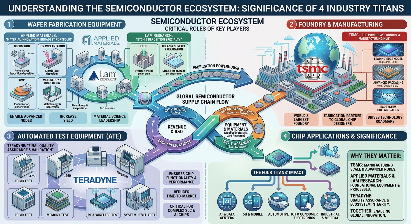
Understanding TSMC, Applied Materials, Lam Research and Teradyne — their technologies, economic significance and strategic relationships
アプライド マテリアルズ、5,000 台目の Producer プラットフォームを出荷 | アプライド マテリアルズ ジャパン 株式会社のプレスリリース
Lam Research Breaks New Ground in Etch Technology and
7
Abstract
The semiconductor industry is one of the most important technological foundations of the modern economy. It supplies the chips that power artificial intelligence (AI), smartphones, computers, telecommunications, cloud computing, banking infrastructure, electric vehicles, industrial automation, medical equipment and modern transportation.
However, semiconductor manufacturing is not the work of a single company. It is a highly interconnected ecosystem in which specialised businesses design chips, manufacture silicon wafers, deposit and remove microscopic materials, inspect structures, and test finished devices.
Four companies illustrate four essential capabilities within this ecosystem:
The true strategic player in the AI era: Why is TSM, with a … – moomoo Community
1. TSMC — The manufacturing engine
Turns customers’ chip designs into physical semiconductor devices at industrial scale.
2. Applied Materials — The materials-engineering specialist
Supplies equipment and technologies used to build, modify and inspect microscopic structures on wafers.
Lam Research Breaks New Ground in Etch Technology and
3. Lam Research — The precision-patterning and materials-removal specialist
Provides equipment for etching, deposition and related wafer-fabrication processes.
聊聊芯片的各类测试:晶圆CP测试、FT测试、SLT测试、可靠性测试、测试设备-电子工程专辑
4. Teradyne — The electronic-testing specialist
Supplies automated systems that test whether semiconductor devices and other electronic components perform correctly.
Central thesis: These four companies occupy different positions in the semiconductor value chain. TSMC manufactures chips, Applied Materials and Lam Research supply important production technologies, and Teradyne helps verify device performance. Their combined significance becomes clearer when we examine the complete journey from silicon to a working electronic system.
Chapter 1. The architecture of the global semiconductor ecosystem
1.1 What is a semiconductor?
A semiconductor is a material whose electrical conductivity can be controlled. Silicon is the most widely used material in mainstream semiconductor manufacturing.
By carefully engineering semiconductor materials, manufacturers create transistors, diodes, memory cells, sensors and other electronic components. Billions of transistors can be integrated into a single advanced processor.
A transistor acts as an electronically controlled switch or amplifier. Large networks of transistors perform calculations, store information and process signals.
The semiconductor ecosystem therefore converts materials, scientific knowledge, engineering equipment and digital designs into electronic intelligence.
1.2 The complete value chain
1. Chip architecture and design
Engineers design processors, memory, logic and circuits.
2. Manufacturing equipment and materials
Applied Materials, Lam Research and other specialist suppliers enable wafer processing.
3. Wafer fabrication
TSMC and other manufacturers build intricate electronic structures on silicon wafers.
4. Electrical testing
Teradyne and other test-equipment providers help identify devices that fail electrical specifications.
5. Packaging and system integration
Chips are packaged, interconnected and qualified for their intended applications.
6. Final products
AI servers, smartphones, vehicles, networking systems and industrial electronics.
This is a simplified map, not a strictly linear sequence. Semiconductor production includes many repeated processing, inspection and testing stages. Testing can occur before and after packaging, and advanced packaging may involve multiple dies manufactured at different facilities.
1.3 The three layers of the ecosystem
| Layer | Main responsibility | Economic function |
|---|---|---|
| Intellectual property and design | Defines what a chip should do | Creates product value and differentiation |
| Manufacturing technology | Supplies equipment, materials and fabrication processes | Makes advanced designs physically possible |
| Production, testing and integration | Manufactures, verifies and assembles devices | Converts engineering designs into usable products |
The four companies you selected illustrate different parts of the second and third layers.
Chapter 2. TSMC — the advanced manufacturing engine
公開台積電工程師的一天 高工時、高強度、高壓力為何撐得住?「台積電之歌」一聽:馬上有PTSD – 今周刊
TSMC Accelerates Arizona Fab Expansion as AI Chip Demand Surges | The Tech Buzz
TSMC releases more details regarding the upcoming 3 nm node – NotebookCheck.net News
8
2.1 Understanding TSMC’s business model
Taiwan Semiconductor Manufacturing Company was founded in 1987 and pioneered the dedicated, or pure-play, semiconductor foundry model.
A foundry manufactures chips designed by other companies rather than primarily competing with those customers by selling its own branded chip designs. This model allows chip designers to concentrate on architecture and product development while relying on specialist manufacturing expertise. TSMC+1
For example, a company might design a powerful AI processor but lack the enormous capital, specialised facilities and process expertise required to manufacture it. It can contract with TSMC to fabricate the design.
2.2 How TSMC turns designs into chips
The production process includes several major stages.
- Design preparation: Engineers prepare the circuit layout and manufacturing data. The design must satisfy the foundry’s process rules.
- Photomask preparation: Patterns are transferred to masks used during lithography, which projects selected patterns onto photosensitive material on a wafer.
- Wafer processing: Repeated cycles of deposition, lithography, etching, cleaning, doping and other processes build transistor structures and interconnects.
- Metrology and inspection: Measurements and defect-detection systems monitor whether the structures meet specifications.
- Wafer-level testing and preparation: Electrical tests identify functional dies, and wafers are prepared for subsequent assembly.
- Packaging and final testing: Individual dies or multiple dies are packaged, interconnected and tested for their intended use.
TSMC performs wafer fabrication and also provides services that include advanced packaging and design enablement. It works with an extensive network of equipment, materials and design-technology suppliers. SEC+1
2.3 Why TSMC is strategically significant
A. Manufacturing scale
Advanced fabrication requires extremely expensive facilities, highly controlled environments, sophisticated process recipes and experienced engineering teams. Scaling a process from experimental production to reliable high-volume manufacturing is a major challenge.
B. Process integration
A chip is not created by one machine. It is the result of hundreds or thousands of interdependent process steps. Small variations can affect performance, power consumption, reliability and the proportion of working chips.
TSMC’s expertise lies in integrating those steps into a repeatable production system.
C. Support for advanced computing
Modern AI processors and high-performance computing chips need large numbers of transistors, fast interconnections, efficient power delivery and advanced packaging. Foundries are essential to converting these designs into manufacturable devices.
D. A platform for innovation
The foundry model allows companies to develop specialised chips without each company having to construct its own leading-edge fabrication facilities.
TSMC’s 2025 annual report describes a global manufacturing business serving high-performance computing, smartphones, automotive electronics, Internet of Things devices and consumer electronics. TSMC+1
2.4 The meaning of nanometres
You will often see semiconductor technologies described using labels such as 7 nm, 5 nm, 3 nm and 2 nm.
These labels are technology-generation names, not necessarily the literal physical length of every transistor feature. Modern transistor geometry is three-dimensional and involves many dimensions, including gate length, spacing and interconnect dimensions.
Smaller technology generations can improve transistor density and energy efficiency, but the benefits depend on the design and process. Manufacturing difficulty and cost also rise in important ways.
2.5 TSMC’s main challenges
- The cost of building and upgrading fabrication plants.
- Maintaining high manufacturing yields as structures become more complex.
- Access to electricity, ultrapure water, skilled workers and specialised equipment.
- Exposure to geopolitical and supply-chain disruptions.
- Balancing demand for advanced chips against the risk of overcapacity.
Conclusion: TSMC is the production integrator. It combines equipment, materials, process knowledge and capital to manufacture chips at scale.
Chapter 3. Applied Materials — engineering the materials inside a chip
アプライド マテリアルズ、5,000 台目の Producer プラットフォームを出荷 | アプライド マテリアルズ ジャパン 株式会社のプレスリリース
Applied Materials Jumps After Solid Q4 Earnings, Bullish Chip Sector Guidance – TheStreet
10
3.1 What does Applied Materials do?
Applied Materials supplies equipment, software and services used in semiconductor manufacturing and other technology markets.
Its semiconductor portfolio covers several major process categories: depositing materials, shaping or removing materials, modifying material properties, analysing structures and enabling connections between components. Applied Materials+1
The key idea is that a transistor is not simply carved out of a solid block of silicon. It is built through carefully controlled sequences of material deposition, patterning, removal, treatment and measurement.
3.2 Five important technology functions
1. Deposition
Adds thin layers of insulating, conducting or semiconductor material. Methods include physical vapour deposition (PVD), chemical vapour deposition (CVD) and atomic layer deposition (ALD).
CMP pad and groove measurement in the semiconductor industry – Novacam
2. Material shaping and planarisation
Helps remove excess material and make wafer surfaces sufficiently flat for subsequent processing.
3. Material modification
Processes such as ion implantation and thermal treatment change the electrical or structural properties of selected regions.
Wafer Defect Inspection System | Optical Surface Inspection
4. Materials analysis and process control
Helps engineers measure critical dimensions, identify defects and monitor whether fabrication remains within specifications.
5. Advanced integration
Supports technologies that connect dies and other structures in advanced semiconductor packages.
These categories describe the broader technology landscape. Not every category uses the same equipment, and not every individual tool is made by Applied Materials.
3.3 Why materials engineering matters
Imagine building a modern city on a microscopic scale.
- Conducting materials act like electrical roads.
- Insulating materials prevent unwanted electrical connections.
- Transistors function as controllable switches.
- Interconnects carry signals between circuit elements.
- Material interfaces influence how reliably the entire structure operates.
The material must be deposited with the correct composition, thickness and uniformity. A layer that is too thick, contaminated or poorly formed can affect electrical performance.
At advanced dimensions, material properties that were once secondary can become central to device performance.
Applied Materials explains that its deposition systems can form films only a few atomic layers thick and that controlling film properties is important for modern devices. Applied Materials+1
3.4 Its significance in AI hardware
AI accelerators require enormous computational throughput and efficient movement of data. Their performance depends not only on transistor count but also on electrical resistance, capacitance, heat, power delivery and interconnect reliability.
Materials engineering can help improve:
- transistor performance and power efficiency;
- the reliability of insulating and conducting layers;
- the dimensions and quality of electrical connections;
- manufacturing yield;
- integration of multiple dies within advanced packages.
Applied Materials is therefore a technology supplier whose equipment helps manufacturers produce increasingly complex electronic structures.
3.5 The business model
Its business is not limited to selling machines. Semiconductor production equipment also requires installation, maintenance, technical support, upgrades and process development.
As manufacturing technology evolves, equipment suppliers work with chipmakers to develop processes that can be repeated reliably in production.
Conclusion: Applied Materials supplies a broad materials-engineering toolkit. Its importance comes from helping manufacturers control the physical properties and structure of the materials that make modern chips work.
Chapter 4. Lam Research — precision etching and nanoscale manufacturing
Lam Research Breaks New Ground in Etch Technology and
感應耦合式電漿蝕刻(ICP-RIE)系統RIE-802iPC|莎姆克股份有限公司
3D NAND Flash – 3D NAND Flash Technology – Illuminating Semiconductors
7
4.1 Understanding Lam Research
Lam Research develops equipment and process technologies used to manufacture semiconductors. It is particularly important in etching and deposition, two complementary processes used repeatedly in wafer fabrication.
Its technologies support the production of logic chips, DRAM memory, NAND flash memory and other semiconductor structures. Lam Research
The fundamental problem Lam addresses is straightforward to describe but extremely difficult to solve: how do you remove or add selected materials with exceptional precision when the structures are incredibly small?
4.2 Understanding etching
Etching is the controlled removal of selected material from a wafer.
Consider a wafer that has a thin film deposited on its surface. Engineers apply a patterned protective layer so that only certain areas are exposed. An etching process removes material from those exposed areas, creating a required structure.
There are different forms of etching, including wet chemical etching and dry plasma etching.
Lam Research is particularly associated with advanced dry etching technologies.
The simplified etching sequence
図解即戦力 半導体プロセスのしくみとビジネスがこれ1冊でしっかりわかる教科書 サポートページ | 技術評論社
Stage 1 — Patterned surface
A thin film is covered by a patterned mask that identifies the areas to retain or remove.
Hide course content | OpenLearn – Open University
Stage 2 — Selective material removal
A controlled process removes material from selected regions while protecting other areas.
Transmission Electron Microscopy of Semiconductors | Thermo Fisher Scientific – US
Stage 3 — Defined structure
The remaining material forms trenches, openings or other structures needed for the device.
These images illustrate the general concept; actual manufacturing uses many more steps and more complex structures.
4.3 What is plasma etching?
Plasma is an electrically energised gas containing charged particles and reactive species. In plasma etching, these particles and chemical reactions remove material from selected regions of the wafer.
The process must control several properties:
- Selectivity: how effectively one material is removed relative to another.
- Uniformity: how consistently the process operates across the wafer.
- Profile control: whether the resulting structures have the required shape.
- Damage control: whether the process affects sensitive underlying materials.
- Repeatability: whether successive wafers meet the same specifications.
Lam’s technical documentation describes plasma etching and atomic layer etching as methods for forming increasingly complex structures with very fine dimensional control. Lam Research
4.4 Why three-dimensional structures matter
Semiconductor scaling is no longer simply about making every feature smaller in two dimensions.
Modern manufacturing increasingly involves complex three-dimensional structures:
- Fin-shaped and gate-all-around transistor architectures;
- vertical layers of memory cells in 3D NAND;
- narrow, deep openings for electrical connections;
- complex interconnect structures;
- advanced packaging features.
These structures create difficult manufacturing requirements. For example, a process may need to create a deep opening without excessively widening its top, damaging its walls or affecting the materials underneath.
Lam’s etch technologies help address these kinds of challenges.
4.5 Deposition: the complementary process
Etching removes material, while deposition adds it. Both are needed throughout fabrication.
Lam supplies deposition technologies as well as etching systems. The specific equipment selected depends on the device architecture, materials and process step.
| Technology | Purpose |
|---|---|
| Etching | Removes selected materials |
| Deposition | Adds controlled material layers |
| Cleaning | Removes unwanted residues and contamination |
| Metrology | Measures dimensions and process results |
| Inspection | Detects defects or unexpected structures |
No single supplier provides every process used in every semiconductor factory.
4.6 Lam Research’s economic significance
Lam is important because complex chips require repeated, highly controlled material-removal and deposition processes.
Its contribution can be understood through four mechanisms:
- Manufacturing capability: enables structures that may be difficult or impossible to produce with less advanced processes.
- Yield improvement: better process control can reduce defects and wasted wafers.
- Product performance: precise structures help determine electrical behaviour and device reliability.
- Production productivity: faster, repeatable processes can increase usable output from expensive factory equipment.
Conclusion: Lam Research is a key specialist in the physical formation of semiconductor structures. It works at the point where material science, plasma physics, chemistry and precision engineering meet.
Chapter 5. Teradyne — the electronic testing and verification engine
AI Drives Higher Demands For Chip Testing
Advanced Automated Probe Systems – MPI Corporation
9
5.1 Understanding Teradyne
Teradyne is a provider of automated test equipment (ATE) and robotics solutions. Its semiconductor testing systems evaluate the electrical behaviour of chips and help determine whether devices meet their specified requirements.
Its broader test portfolio also serves wireless, automotive, industrial, computing, communications and other electronic applications. SEC
The essential distinction is that manufacturing creates the device; testing provides evidence about whether the device performs correctly.
5.2 Why chips must be tested
A chip can look physically correct and still fail electrically.
Possible causes include:
- defects introduced during fabrication;
- unexpected electrical leakage;
- faulty transistor or interconnect behaviour;
- timing or signal-integrity problems;
- excessive power consumption;
- faults introduced during packaging.
A modern semiconductor may contain billions of transistors. Checking every transistor individually with a separate manual measurement would be impractical for high-volume production.
Automated testing uses specialised hardware and software to apply electrical signals, measure responses and compare results against defined limits.
5.3 How automated semiconductor testing works
Test program
Defines the signals, measurements and acceptance criteria.
Automated test equipment
Generates electrical inputs and measures device responses.
Chip or wafer connection
Connects the tester to the device through suitable probes or test interfaces.
Measured results
Electrical responses are evaluated against specifications.
Pass
Meets the tested criteria.
Fail
Does not meet one or more criteria.
A pass means that the device met the specifications covered by that test. It does not mean that every conceivable fault has been ruled out.
5.4 Major testing stages
A. Wafer sort
Individual dies on a wafer are tested before they are separated. This helps manufacturers identify dies that fail the applicable electrical tests.
B. Final packaged-device testing
After packaging, the device is tested again. The procedure may check functionality, performance, power consumption and other requirements relevant to the chip.
C. System-level and application-specific testing
Some products require further validation under more representative operating conditions, particularly where reliability and safety are important.
Teradyne’s exact role depends on the customer, product and test stage. Other test-equipment companies and in-house systems also participate in this market.
5.5 Why Teradyne matters for AI chips
AI processors are demanding devices. They may contain many processing units, high-speed interfaces and complex power-management systems.
Testing can help evaluate:
- logic functionality;
- memory and interface behaviour;
- timing and operating speed;
- electrical power characteristics;
- defects and manufacturing variation;
- whether a device meets its intended operating specifications.
As chips become more complex, test programmes and equipment must keep pace with growing requirements for test coverage, throughput and measurement accuracy.
5.6 The relationship between testing and yield
Suppose a hypothetical factory produces 10,000 dies.
- 9,000 meet the required manufacturing and electrical criteria.
- 1,000 fail at least one criterion.
The initial pass yield in this simplified example is:
\[ \text{Yield}=\frac{9,000}{10,000}\times100=90\% \]
Testing does not automatically repair the 1,000 failing dies. Instead, it identifies failures, prevents unsuitable devices from being treated as conforming products, and generates information that engineers can use to investigate manufacturing problems.
Conclusion: Teradyne supplies a crucial verification capability. Its equipment helps manufacturers measure the electrical quality and performance of devices before those devices enter larger electronic systems.
Chapter 6. Comparing the four companies: who does what?
The most important distinction is that these companies do not perform the same job. They contribute different capabilities to the semiconductor ecosystem.
TSMC Accelerates Arizona Fab Expansion as AI Chip Demand Surges | The Tech Buzz
TSMC — manufactures chips
Foundry
Primary contribution: integrating complex manufacturing processes to turn customer designs into physical semiconductor devices.
Key measures: yield, performance, cost per wafer, production capacity and delivery reliability.
Applied Producer XP Pioneer CVD
Applied Materials — engineers materials
Equipment supplier
Primary contribution: broad technologies for depositing, modifying, shaping, analysing and integrating materials.
Key measures: film quality, process control, equipment productivity and customer process performance.
Lam Research — shapes microscopic structures
Equipment supplier
Primary contribution: specialised etching and deposition technologies for intricate semiconductor structures.
Key measures: etch precision, selectivity, uniformity, repeatability and wafer throughput.
Teradyne Introduces the UltraFLEXplus to Minimize Time to
Teradyne — verifies electronic performance
Test-equipment supplier
Primary contribution: automated testing systems that measure device behaviour and identify failures against specified criteria.
Key measures: test coverage, measurement accuracy, test time and cost per tested device.
The company roles described above are based on their published business and technology descriptions. SEC+3
Chapter 7. How the four companies fit into one technological system
Imagine that a chip designer wants to develop an advanced AI processor.
The process below explains the relationship between the four businesses without suggesting that every chip passes through a fixed sequence of equipment from these four companies alone.
AI Processor on a Green Electronic Circuit Board
Step 1 — A chip is designed
A designer specifies the processor’s architecture, logic, memory interfaces and electrical requirements.
Building on an Unmatched Foundation of CVD Innovation
Step 2 — Materials are engineered
Applied Materials and other equipment suppliers provide tools for forming and controlling the required material layers.
Step 3 — Structures are patterned
Lam Research and other suppliers provide etch and deposition technologies used to create intricate device structures.
TSMC Accelerates Arizona Fab Expansion as AI Chip Demand Surges | The Tech Buzz
Step 4 — The foundry integrates production
TSMC combines the required equipment, materials, process recipes and manufacturing controls to fabricate chips.
AI Drives Higher Demands For Chip Testing
Step 5 — Devices are tested
Teradyne and other test-equipment providers supply systems for checking electrical performance and identifying failures.
AI Cluster Solutions for Scalable Compute | Hypertec
Step 6 — The chip powers a system
After appropriate packaging and integration, the processor can be deployed in an AI server or another electronic product.
An important technical distinction
Applied Materials and Lam Research are equipment suppliers to manufacturers, not interchangeable chip foundries. They also compete with other equipment suppliers in certain categories.
TSMC is a foundry that uses equipment from multiple vendors. Teradyne supplies testing equipment to semiconductor and electronics manufacturers; it is not simply the last step in every TSMC production line.
The relationship is best understood as an interconnected industrial ecosystem, not as a partnership in which all four companies necessarily work on every individual chip.
Chapter 8. The economic significance of the four companies
8.1 Their role in the artificial intelligence economy
AI depends on more than software algorithms. Large-scale AI systems require advanced processors, memory, networking, electrical infrastructure, cooling and reliable manufacturing.
TSMC: computing supply
Its manufacturing capabilities help turn high-performance computing designs into chips used in AI accelerators and related systems.
Applied Materials: material innovation
Its equipment supports the production of complex layers and structures that influence transistor performance, power and reliability.
Lam Research: structural precision
Its technologies help manufacturers create the intricate features needed for modern logic and memory devices.
Teradyne: product verification
Its testing equipment helps manufacturers determine whether chips satisfy electrical and performance requirements.
8.2 Productivity and economic value
The semiconductor ecosystem creates value by allowing a large number of specialised organisations to focus on their strongest capabilities.
A foundry can concentrate on manufacturing. Equipment suppliers can invest in developing specialised process tools. Chip designers can focus on architecture, software compatibility and product differentiation.
This division of labour can reduce duplication of investment and support technological progress.
However, it also creates dependencies: a disruption affecting a critical material, piece of equipment or manufacturing facility can influence companies much further down the value chain.
8.3 Employment and industrial development
The ecosystem supports highly specialised work in:
- electrical and electronic engineering;
- materials science and chemistry;
- physics and applied mathematics;
- mechanical and mechatronics engineering;
- computer science, software and automation;
- quality assurance and statistical process control;
- supply-chain management, finance and industrial operations.
For countries seeking to expand their technology industries, semiconductor-related opportunities include equipment maintenance, electronics testing, design services, industrial software, component distribution, research and technical training. Building a leading-edge wafer fab, however, requires much greater capital, infrastructure and technical capability than many supporting businesses.
Chapter 9. Risks, competition and strategic dependencies
Understanding these companies requires examining not only their technology but also their operating risks.
| Risk | Potential effect |
|---|---|
| Semiconductor demand cycles | Equipment orders and chip demand can fluctuate sharply. |
| Manufacturing complexity | Process failures can reduce yield and raise production costs. |
| Capital expenditure | New fabrication capacity requires large investments before revenue is generated. |
| Export restrictions | Rules governing advanced technology can affect access to equipment and markets. |
| Geographic concentration | Disruptions in key manufacturing regions can affect global supply. |
| Customer concentration | Dependence on a small number of large customers can increase business volatility. |
| Technology transitions | Companies must invest continuously to keep their products and processes competitive. |
Why equipment companies can experience different business cycles from foundries
When a foundry expands a factory, it buys manufacturing equipment. Once the factory is installed, equipment spending may slow even if chip production remains strong.
Conversely, when manufacturers begin preparing for a new technology generation, they may increase equipment investment before the resulting chips reach high-volume production.
Therefore, TSMC’s manufacturing demand and the equipment demand experienced by Applied Materials and Lam Research do not necessarily peak at the same time.
Teradyne’s business can also respond differently because test-equipment demand depends on device complexity, test intensity, customer investment and the volume of products being tested.
Chapter 10. Understanding the companies through an economic framework
A useful way to analyse these businesses is to separate the technology function from the economic function.
| Dimension | TSMC | Applied Materials | Lam Research | Teradyne |
|---|---|---|---|---|
| Main business | Chip manufacturing | Process equipment | Process equipment | Automated testing and robotics |
| Main customer need | Reliable production at scale | Material and process control | Precision material processing | Electrical verification |
| Main technical challenge | Integrating many process steps | Engineering material properties | Forming complex structures | Accurate, efficient testing |
| Principal economic driver | Wafer demand, process leadership and yield | Equipment investment, service and technology adoption | Equipment investment, process transitions and service | Test-system demand, chip complexity and test requirements |
| Position in value chain | Manufacturing | Manufacturing technology | Manufacturing technology | Testing technology |
These are analytical categories, not a ranking of the companies. Their revenue, profitability and competitive positions must be evaluated using their individual financial statements and current market conditions.
Chapter 11. A practical framework for evaluating the four companies
If your objective is to understand their industrial importance or study their business performance, consider these five questions for each company.
- Technology leadership: What specific engineering problem does the company solve, and how difficult is it for competitors to reproduce its solution?
- Customer dependence: How concentrated are its customers, and how important is its technology to their operations?
- Revenue quality: How much revenue comes from equipment sales, recurring services, upgrades or other business activities?
- Investment requirements: How much capital and research expenditure are required to maintain technological competitiveness?
- Industry outlook: How might AI, memory demand, advanced packaging, new manufacturing processes and geopolitical developments affect the business?
These questions provide a stronger foundation for understanding the companies than simply assuming that all semiconductor-related businesses benefit equally from AI growth.
Chapter 12. Glossary of essential semiconductor terminology
| Term | Simple explanation |
|---|---|
| Semiconductor | Material whose electrical conductivity can be controlled. |
| Integrated circuit (IC) | Electronic circuit containing interconnected components on a chip. |
| Wafer | Thin, circular substrate on which many chips are fabricated. |
| Foundry | Company that manufactures chips for customers. |
| Fabrication plant (fab) | Facility in which semiconductor wafers are processed. |
| Lithography | Process for transferring patterns onto a wafer. |
| Deposition | Adding a controlled layer of material. |
| Etching | Selectively removing material to form a structure. |
| Metrology | Measuring dimensions and physical properties. |
| Yield | Proportion of units meeting defined acceptance criteria at a particular production stage. |
| ATE | Automated test equipment used to measure device performance. |
| Advanced packaging | Techniques for connecting dies or components into a more capable semiconductor package. |
| Capital expenditure | Money invested in long-lived assets such as factory equipment. |
| Process node | A label for a semiconductor manufacturing technology generation. |
Conclusion: Four specialised capabilities, one semiconductor ecosystem
The semiconductor industry advances through the combined work of designers, foundries, materials scientists, equipment engineers, test specialists and many other organisations.
- TSMC turns complex chip designs into manufactured silicon.
- Applied Materials supplies broad technologies for engineering and controlling materials.
- Lam Research supplies specialised technologies for etching and depositing the structures inside chips.
- Teradyne supplies automated testing systems that help verify electronic performance.
Their importance comes from the specialised problems each solves and the way those capabilities fit into the wider production system. None can be understood fully in isolation from the designers, suppliers, manufacturers and customers around it.
For anyone studying modern technology and the economy, the key lesson is that a semiconductor is not simply a piece of silicon. It is the outcome of an enormous coordinated system of science, precision engineering, industrial investment, software, manufacturing discipline and quality control.
Further reading: primary company sources
TSMC
Official company mission, manufacturing model and annual reporting.
Company mission · Investor relations
Applied Materials
Equipment technologies and semiconductor process categories.
Lam Research
Etch processes and precision semiconductor manufacturing.
Teradyne
Automated test systems, semiconductor testing and robotics.




Be First to Comment